Methods to increase voltage margin of a signal by mitigating the effect of previous bits on a given bit.
Decision feedback equalization (DFE) is becoming increasingly popular for high-speed digital circuits. This form of equalization has been around for a while in the SerDes world, where it is standard for protocols such as PCIE-G3. The equalization scheme is now also working its way into the world of DDR, where DDR5 is slated to incorporate DFE in DRAMs.
What is DFE, and how does it work? The following is an attempt to highlight an intuitive approach for understanding DFE.
The concept behind DFE is rather simple. To put it in a sentence, DFE tries to compensate for the bad behavior of the previous bits. Seen another way, it tries to clean up the effects of a given bit on subsequent bits.
To understand this better, let’s start by thinking about a channel where the transmitter sends a series of 0s, a single 1 and another series of 0s. In this hypothetical channel, it is possible, due to the characteristics of the transmitter and the channel, that the signal just doesn’t have the time or the slew rate to reach the reference threshold at the receiver to be registered as a 1. In this case, as shown in FIGURE 1, the receiver won’t receive what was transmitted because it doesn’t cross Vref.
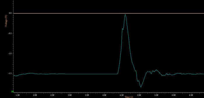
Figure 1. High going pulse not crossing threshold.
Now, if the Rx knows that the previous bit was a 0, and so knows the voltage will be low, it can artificially boost the voltage internally – or equivalently lower the Vref threshold (FIGURE 2). It effectively gives a helping hand to a signal it knows has to work extra hard to make it to a 1 state, since it’s starting from such a low state. By doing this, the bit will be able to correctly be interpreted.
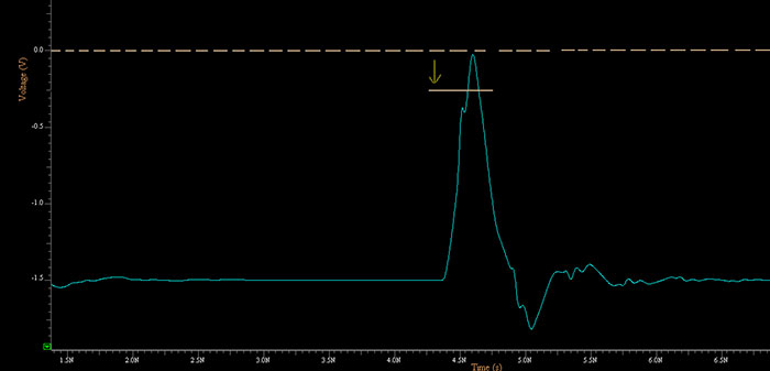
Figure 2. High pulse crossing threshold by lowering threshold.
Now what if, instead of a 1, the bit remained at 0? That’s really not a big problem because the signal will simply remain below the Vref threshold, continuing to be interpreted as a 0. In other words, for a small margin loss of interpreting a 0, there will be a great boost in interpreting a 1.
DFE 101. What we just saw is a “1-tap” DFE. This means the DFE will adjust the current waveform (or the reference voltage) based on what the previous bit was. In this example, if the previous bit was a 0, then either the signal’s voltage will artificially be increased, or the Vref will artificially be lowered (same effect, implementation might be chip-specific). This 1-tap DFE is often represented as the block diagram in FIGURE 3.
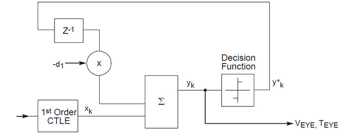
Figure 3. 1-tap DFE block diagram.
An easy way of understanding this block diagram is to start the analysis from y*k (near the right of the diagram) rather than the left-hand input. This is the bit value the DFE slicer has estimated the bit to be: either a +1 (corresponding to a high) or a -1 (corresponding to a low).
This bit then gets delayed by one UI through the delay block z-1. This delayed bit is then multiplied by the DFE value, and the product added to the incoming signal. This DFE value is the amount of adjustment made. Note this value is negative. If the bit at y*k is negative (i.e., the bit was a 0), then the product with the negative DFE value will yield a positive number, effectively increasing the voltage of the subsequent bit. If the bit at y*k is positive (i.e., the bit was a 1), then the product with the negative DFE value will yield a negative number, effectively decreasing the voltage of the subsequent bit.
In the example shown in Figures 1 and 2, the reference voltage is shifted by an amount equal to the DFE value. In this block diagram, it is the actual voltage that is being shifted, rather than the reference. Shifting the voltage or shifting the reference is just an IC implementation detail; shifting the reference one way has the same net effect as shifting the voltage the other way. After all, once they get to the comparator/slicer, it doesn’t really matter whether one moved up or the other moved down. It’s only the relative voltage that matters.
DFE 201. Now let’s extend this to two bits. The same basic logic applies. The aim is to mitigate the impact of the previous two bits on the current bit. If the previous bit was 0, and the bit before was also a 0 (i.e., “00”), then the current voltage can be expected to be at a certain bias, which is different from a 1 followed by a 0 (i.e., “10”).
As an example, we can take the case of the previous two bits being “10,” and the current bit being a 0. Let’s say the response of the “10” is as shown in FIGURE 4. In this case, the current bit (highlighted with the arrow as the third bit in Figure 4) will be biased by about 400mV. If the threshold is 750mV, then that leaves only 350mV of margin if the current bit is a 0. In this case, the DFE design can adjust the voltage lower (or the Vref higher) during the sampling point of the current bit (i.e., the bit after the “10” bit pattern) to compensate for the signal’s behavior to provide a larger margin.
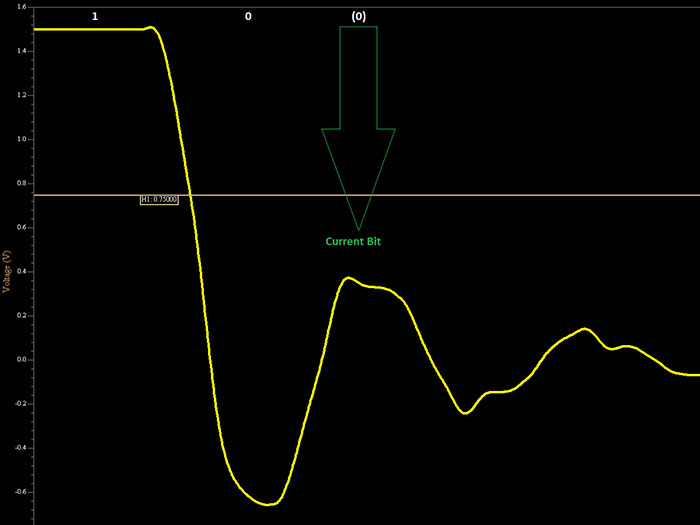
Figure 4. Example of previous pulse on current bit.
This concept can be extended further to incorporate more bits. Each additional bit before the current bit that needs to be considered requires an extra “tap.” Seen another way, the number of DFE taps needed is at least equal to the number of UIs that a given symbol’s energy remains in the channel. The number of Taps in the DFE system, therefore, indicates the number of prior bits whose effects are mitigated on the current bit. The number of taps in the DFE needs to be sufficient to incorporate the effects of ISI until it dies down to an acceptable level. For example, if a transition’s energy stays in the channel for 5UI before attenuating to an acceptable level, then at least a 5-tap DFE is recommended. Regardless of the number of taps, the intent remains the same: to compensate for any sequence of previous bits to nullify their impact on the current bit.
After a certain time, the effect of the “old” bits doesn’t matter so much to the current bit. The effect would have mostly died away. So, adding more DFE taps won’t result in a significantly larger benefit. This is important because DFE can consume a significant amount of power and silicon real estate. Using fewer DFE taps can help lower total power requirements of the setup.
Advantage and drawbacks. One key advantage to DFE over other linear equalizers is that noise is not amplified along with the signal. Because the voltage shifting is based solely on the determined digital values, there is no amplification of the noise that is superimposed on the signal. This permits DFE equalizers to be effective in situations where linear equalizers might not.
Because DFE uses the digital bits from the sequence, and because these bits are determined based on the signal voltage at the sampling point being compared with the threshold, there is a possibility due to noise that the bit gets incorrectly assessed. When this happens, it might cause the voltage shifting to happen in the wrong direction, potentially causing a cascade of subsequent incorrect decisions.
DFE can offer a method to increase the voltage margin of a signal by mitigating the effect of previous bits on a given bit. The number of previous bits’ effects mitigated depends on the number of taps in the equalizer. However, since each tap is expensive both in terms of silicon real estate and power, the number should be limited to as many as is realistically expected in the system. By using an optimal number of DFE taps, information from signals can be recovered, which might be difficult using linear equalizers. Finding the optimal number of taps, and the values to be used for those taps, can be addressed using simulation tools.
Nitin Bhagwath is product architect at Mentor, a Siemens business (mentor.com); This email address is being protected from spambots. You need JavaScript enabled to view it..


