In PDN design, maintain a low impedance over a range of frequencies, as opposed to just one.
Achieving a robust and functioning power distribution network isn’t difficult if we provide both the capacity and responsiveness needed at each device. Previous columns addressed capacity concerns, discussing the need for sufficient copper (or an alternative conductor) between a voltage source and any load depending on it for its supply. Here, we build on those and examine what’s required to maintain that network at a steady voltage. This relies on sufficient “energy stores” and the conduction paths needed to deliver charge quickly to any location on the board experiencing “instantaneous demand.”
DC vs. AC (aka static vs. transient). Historically, nearly all power conversations pertaining to printed circuit boards have been lumped into two categories, with the terms “power DC” and “power AC” emerging as almost standard terminology. Power DC is understandable as it addresses PDN capacity issues associated with inadequate copper.
Our experience with DC analysis reveals the simulation process, once thought to be complex, is nothing more than the visualization of Ohm’s law. With voltage defined in our DC supplies, and current by the operating requirements of each load, we found tools could readily calculate the resistance by extracting the geometry of the conductors. Using these resistance models in conjunction with the current needs of each IC (defined by their electrical specifications), it is easy to predict the DC voltage available in each chip given its distance from the source. This makes the cumulative resistance from the source the determining factor defining the DC performance each IC experienced.
To continue reading, please log in or register using the link in the upper right corner of the page.
Read more: Meeting On-time Power Requirements All the Time
Chip caps help only if the conduction in the path is sufficient to deliver the right charge.
Much of the talk in the simulation world lately is focused on power. Even SI experts are starting to see how power has a material impact on their high-speed data transfer success. With power on the forefront, what effect will that have on the additional design demands of low-frequency supplies? Why should you consider power throughout your design process?
Signal integrity, at its basic core, studies and describes the effects physical structures have on a signal, as it is transmitted from a source (transmitter) to a destination (receiver), but makes no mention of where the energy for the signal originates, or where it goes once received. Although a bit of oversimplification, the transmitting IC pulls energy from its power supply, bundles it as a bitstream and transmits data to a receiving IC, where the energy is dumped onto the ground and eventually returns to the power supply, ready to repeat. Admittedly, today’s high-speed signals are largely differential and draw from multiple power rails, so we aren’t describing the exact current flow. What we are describing is the notion that reliable data transmission involves both a clean path from driver to receiver in addition to a well-designed plan to deliver and return needed power.
In our previous column related to power distribution (PCD&F, April 2021), we discussed capacity. Specifically, we focused on the increasing current demands associated with most new designs and showed the need to ensure our conductors (pins, planes, vias, and etch) were up to the challenge. Today we add another requirement: responsiveness. Even an IC with ample current supply could experience “power shortage” if the energy needed to transmit the data bitstream isn’t available in time.
To continue reading, please log in or register using the link in the upper right corner of the page.
Two compelling forces driving much of our technology – miniaturization and performance – are not new. In fact, one could say they have appeared within every product spec and design document in some form or another since the terms were coined. Fundamentally, this has enabled capability and portability with products in virtually every hardware sector. This will (and should) continue. In the area of miniaturization, both board and package are transforming as technologies such as rigid-flex, blind/buried vias, and multi-die packages move from fringe to mainstream. Further, performance improvements maintain the well-known doubling trajectory and are propelled forward by orders of magnitude in speed, while increasing efficiency and extending battery life. Often these gains are continually achievable only by reducing the voltage swing to under a volt. As miniaturization and performance drive devices to new functionalities and applications, the effects of these requirements are visible throughout the design process. Nowhere is this drive for smaller, faster, cheaper more noticeable than in power.
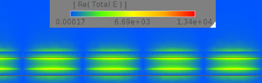
Power demands outpacing supply. To comprehend the extent of the power delivery network (PDN) transformation, consider the following. Design requirements associated with power delivery have become substantially more complex, with many ICs requiring power to be supplied at multiple voltage levels. Frequently those levels are near or below a single volt, contracting virtually every threshold and reducing margins to mere millivolts. Simultaneously, demand for current has skyrocketed in some product areas, made obvious by the extent to which we now account for adequate cooling. In addition to these increased electrical demands, the PDN must also be more responsive, capable of supplying the instantaneous current demands of high-speed signaling. While all this may suggest a more robust PDN is needed, as many new products reach manufacturing, often the opposite is true. Not surprisingly, the miniaturization effort has had a consolidating effect on the physical hardware, frequently bringing high-current ICs closer together (FIGURE 1). Advances in device packaging have contributed as well. Pin counts can easily exceed a thousand on a single package, and mainstream spacing under a millimeter contributes to the same reality: The PDN is comprised of less copper in today’s PCB than it was just a few years ago.
To continue reading, please log in or register using the link in the upper right corner of the page.
Read more: DC Analysis: Keeping PDN Running Smoothly (Not So Easy Anymore)
Assumptions made in simulation may not reflect live board conditions.
As simulation and analysis continue to mature, the evolution is from a mechanism for finding problems to a methodology for preventing them. Many design teams have advanced beyond checking for violations and now use the tools to make informed design decisions early in product development. This results in better products reaching production floors despite condensed schedules.
Chasing correlation. With increasing reliance on simulation and analysis comes the responsibility to understand the capabilities and limitations of these tools. While able to calculate remarkably accurate results, they do rely on some basic assumptions. Not long ago, the “via” was assumed to be a plated hole extending the full thickness of the circuit board, resembling a coaxial cable, and could be sufficiently modeled as such. The drive for miniaturization and advances in manufacturing revolutionized this structure, introducing laser drilling, buried and blind, nested, and stacked constructs that quickly invalidated the coaxial cable model. Now they can be modeled in detail using 3-D solvers. Design teams, likely aided by simulation, recognized the via as the single structure in the signal path that presented both the greatest threat to signal integrity and the largest contributor to discrepancies between simulation and measurement. Had we not challenged the assumptions made regarding the via, simulation and measurement would continue to diverge as complex via structures became mainstream. Instead, traditional simulation, aided where necessary with 3-D electromagnetic field solvers, continues to produce results predictive of the actual measured product.
To continue reading, please log in or register using the link in the upper right corner of the page.
Read more: The Rise of Power Integrity Analysis for Designers