With many disciplines contributing, who will manage the process?
As technology trends toward smaller, faster, cheaper, the challenges around good PDN design get more difficult. With multiple requirements needed from many disciplines, the PDN’s demands will only increase and become harder to maintain.
Over the past few months, we have discussed elements essential to power delivery and PDN requirements. Now that we have a better understanding of this, it’s time to explore what is needed to create the ideal PDN product, and who is best equipped to bring together all the elements of the PDN.
What is a good PDN design, and how do you achieve it? Power-related design objectives tend to be similar in nature for all PCBs: to provide sufficient current at a stable voltage to each device. What does vary widely is complexity, however. Said objectives can range from simple single-supply, powering a solid power plane, to a multi-source, hot-swappable, self-monitoring, thermally sensitive, complex design that accounts for most components and a large amount of copper on the PCB. Simply put, good PDN design delivers power adequately and reliably.
To continue reading, please log in or register using the link in the upper right corner of the page.
Understanding cap differences and modeling will help identify loop inductance issues early.
We’ve written for months about how to control power delivery. While we have learned the effects of layout on the PDN, we haven’t yet focused on the other major influencing factor: the decoupling capacitor.
These simple, 2-pin devices perform two main tasks: resist a change in voltage across their pins and accumulate and store “charge” that can be delivered from those pins to maintain that voltage. In the world of digital design, this “decoupling” function is huge and is arguably why we do power integrity (PI) simulation in the first place. The power demands of a product’s components are largely defined by its features and performance requirements, which determine supply sizes. Between those lies the power delivery network (PDN), a subject we’ve intensely studied. Composed almost entirely from capacitors and the copper that connects it all together, the success or failure of a PDN is often determined in layout. In previous articles, we’ve written about “loop inductance” and how it impacts the capacitors’ ability to do their job. A solid understanding of cap differences and modeling will help identify loop inductance issues early to ensure a successful PDN.
To continue reading, please log in or register using the link in the upper right corner of the page.
Read more: PDN Effectiveness: The Devil’s in the Decap Details
We’ve discussed the importance and care required when routing the power delivery network (PDN) of modern printed circuit boards. From how to support current supply needs, loop inductance, and defining layer stack-ups, it may seem we’ve addressed all the power concerns one could have. This is just a fraction of the considerations a designer needs to keep in mind, however. The PDN has an important secondary role that has nothing to do with power delivery. Often forgotten, the PDN is responsible for roughly 50% of the conduction avenues for the non-power signals.
Commonly referred to as return path, this routing “completes the loop,” enabling current to flow. It can be as influential (and problematic) to signal quality as the transmission lines we study in detail. In fact, failure to address the return path is a leading cause of signal integrity issues. Perhaps more troubling, they frequently go undetected even in the setting of comprehensive simulation.
To continue reading, please log in or register using the link in the upper right corner of the page.
Read more: Your PDN’s Other Job: Closing the Loop with the Return Path
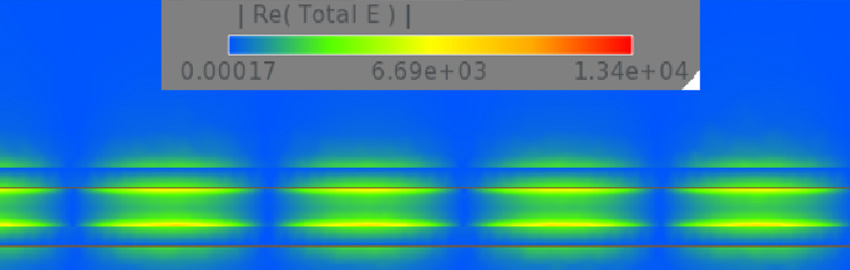
Fast interfaces and switching speeds are becoming commonplace, and with them comes increased noise, amplifying any problems within the power delivery network. Products today are the direct result of the fast signal capabilities in current technology, making it impossible to eliminate noise. This noise can be seen in the form of simultaneous switching noise, which resonates and can combine to destroy the voltage signal and collapse the signal eye. Therefore, the only viable option is to mitigate the noise via containment.
Ground is the point from which every measurement is evaluated. Therefore, any variation will affect timing and voltage. Every signal switching on the board, whether slow or fast, contributes to noise on the power and ground planes. This “ground bounce” is commonly referred to as simultaneous switching noise (SSN) and is essentially crosstalk on the ground (FIGURE 1).
To continue reading, please log in or register using the link in the upper right corner of the page.