Prepping the data for placement and soldering.
In part one of this two-part series on assembly data and documentation, we discussed how data drive the assembly package and listed several items needed for it to be complete. Understanding this and the manufacturing process will help users make sound design decisions. This column provides a deeper dive into each step of this process.
Programming the placement machinery. Once the parts (including the PCB panels) are purchased, the automated assembly process can begin. Data required for this phase of the manufacturing process are taken from a few valuable sources. For the manufacturing engineer, the bill of materials (BoM) provides a limited view of the requirements. Along with the BoM output, the designer has hopefully provided an intelligent data format file for the design. With this information, the manufacturing engineer can get a good look at the design intent and begin planning the order of manufacturing operations.
The provision of x, y placement data output from the design database is invaluable to the process. Sometimes referred to as a “pick-and-place” file, the data can be fed into process programming to help select the proper tape reel and define the nominal location and rotation for each SMT part that will be automatically soldered to the board.
If there are SMT parts on both sides of the board, the placement file will indicate this, and the placement parameters will be divided into two operations (called first pass and second pass) to place and solder SMT parts to their respective sides.
All remaining through-hole parts which are not to be run in the reflow oven process will be designated for secondary solder processing. This can be performed manually by a soldering technician or by two other common automated processes: wave soldering and selective soldering.
Assemblers widely use wave soldering to make solder joints on the side of the PCB from which the through-hole pins protrude. The best-case condition for wave soldering is when all the parts are mounted on the topside of the PCB. Only the through-hole pins needing solder and the secondary side of the PCB should meet the solder wave (FIGURE 1).
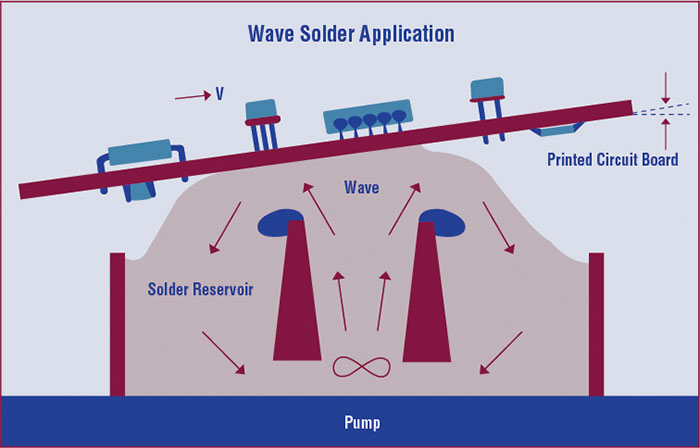
Figure 1. Wave solder application process.
When SMT exists on both sides of a mixed technology PCB, it is far more common to process both sides of the PCB SMT passes in the reflow oven. Then, the assembler selectively solders the remaining through-hole parts on the assembly.
Selective solder machinery can make accurate solder joints on through-hole component pins by positioning a small fountain of solder underneath the selected pin and automatically raising the fountain cup to a height to make the solder joint (FIGURE 2). The process is highly accurate but is not considered “speedy” due to the nature of the single solder fountain head.
Figure 2. Example of how the selective solder process works.
Many important decisions must be made regarding solder processing before a board begins to roll down the assembly line. Although the assembler has many options to address the manufacturing challenges, the PCB design engineer’s goal should be to communicate with the manufacturing engineering stakeholder. Seek out design solutions to reduce these multiple process requirements as much as possible; that’s just good DfM.
Automated placement. After solder paste is applied, the panel moves onto the placement line. The panel is designed to include rails, which not only provide stability to the panel structure, but support the panel on the conveyer as the panel is moved into position for automated placement. The pick-and place machine optically calculates the exact position and rotation of the panel. The PCB designer provides the coordinate starting point of the panel via the placement file,
permitting the machine to place components on the panel with lightning speed.
Moving through the reflow oven. Once all the parts are placed on the side to be assembled, the panel moves along the conveyor into the reflow oven, where the assembly is heated, the solder melted, and solder joints formed.
A few variables must come together well for solder joints to be in spec:
- The footprint land geometry must be designed properly with enough toe and heal and side extension to permit a perfect solder fillet. (See IPC-7351 for more information.)
- The optimal amount of solder paste must have been applied to the land by accurately calculating the stencil opening in relation to the stencil thickness and the type of solder used on the PCB.
- The oven’s thermal profile (or heat zones) must be optimized so the PCB and components receive the proper thermal ramp, soak and cooling times to permit the solder to flow and solidify properly.
Second operation assembly processing. As mentioned, parts not suitable for reflow must be processed using different manufacturing practices. It is usually up to the manufacturing engineer to determine how these remaining components will be soldered. The PCB assembly drawing the designer provides should specify the components be “soldered” without being specific as to how. This is for manufacturing flexibility. Some through-hole parts must be addressed specially with alternative soldering processes such as wave and selective soldering, but many other types of assembly actions are required on the PCBA after all the parts are soldered. It is important for these second-op conditions to be carefully considered by the PCB designer during the layout phase, hopefully in collaboration with the manufacturing engineering stakeholder. Ultimately, it is up to the design and engineering stakeholders to define the performance requirements of the product. Ideally, it is left to the manufacturer to decide how to accomplish them.
Assembly test. Once all the assembly operations and processes have been run, verification must take place for the PCB assembly to be validated for performance. This is the point where all the frontend investment of time and expense to add test points and create fixtures and software mentioned in our column on design for test is going to pay off. If everything has gone according to plan, the PCBAs are taken from the line and placed into the assembly test fixture. There is a program to check for continuity between parts to ensure all the soldering and placement has gone smoothly. Functionality checks will supply power to light LEDs and run displays. The test engineers have collaborated with the PCB design engineer to make certain every function of the PCBA is tested and performs within specifications.
If a problem is found, such as a mislocated part or even an incorrect part, the board can be set aside for rework. After rework, the board will have to run through the entire assembly test process again to ensure complete conformance.
Final inspection (IPC-A-610). A few assembly notes may be deemed necessary on an assembly drawing. Adding a simple note, “Acceptance criteria per IPC-A-610,” says all the right things to the final inspection department. The pictorial, easy-to-read specification covers conditions of every basic process the PCBA will have been exposed to during its journey through the assembly shop.
IPC-A-610 and the many other specifications utilized to compare manufactured hardware with conforming or nonconforming criteria are invaluable guidelines for final assembly test technicians to measure how each stakeholder has done their job. Once all the solder joints and parts are inspected, and the PCBA has passed burn-in testing, the manufacturing process is complete, and the PCBA is ready to be shipped.
Conclusion. Within the PCB assembly process or any PCB-related process, tens of thousands of things can go wrong. The fully engaged stakeholder knows the processes inside and out and has learned from each assembly, each cycle, and has made the required adjustments. So must the PCB design engineer. Data and documentation created by the PCB design engineer on the frontend must be clean: garbage in equals garbage out.
Every topic and character description throughout this series illustrates a relative interconnectivity between stakeholder responsibilities and the design manufacturing and assembly processes. It is the hope of all the contributors of this series that its message of collaboration, communication, and understanding will serve the designer well, as they assume an influential role as the hub of the entire design and manufacturing process for the PCBA. Learn from your assembly manufacturing colleagues to incorporate the tangible causes of success into your own PCB design process.
This excerpt of The Hitchhiker’s Guide to PCB Design was written by EMA Design Automation with Patrick Davis of RocketEMS. Download to learn more about PCB design stakeholders and real-world, actionable PCB design tips from industry experts (go.ema-eda.com/pcbguide).
Register now for PCB West, the leading conference and exhibition for printed circuit board design! Coming Sept. 9-12 to the Santa Clara Convention Center. pcbwest.com


