Route the critical nets first.
Last month, we established the PCB stackup is more than just a thickness diagram. This lays the foundation for routing and utilization of copper planes within the layout. There are five important topics to consider during completion of the layout:
- Design rules
- Defining vias
- Utilizing planes and pours
- Impedance control and signal integrity
- Routing
Design rules. To successfully complete a PCB layout, set the design rules to match the estimated producibility class of the design. PCB design rules can be set in most layout tools that permit generic settings to be saved. Design rules checking (DRC) tools will examine against these rules in real-time, providing instant feedback. Having this real-time feedback is invaluable as a designer. Trying to track all the rules and how they interrelate manually is not a task you want to take on.
Just about everything pertaining to copper in a PCB design is controllable in the design rules portion of a PCB layout tool. The preset design rule values or “default settings” are established by an EDA provider that knows nothing about the specific layout a designer may be working on. Hundreds, if not thousands, of control variants in the tool’s default settings can cause catastrophic manufacturing conflicts if not reset to match the requirements of a new project.
Once the connectivity of the layout is synchronized with the schematic, surmise which general design rule constraints will best control the new design and reset them for the required result (FIGURE 1).
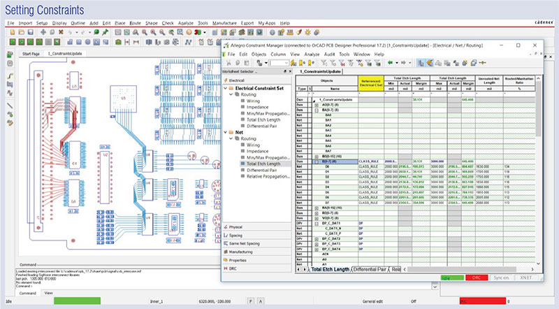
Figure 1. Setting constraints.
In general, five basic areas will need to be configured to match the design being worked on. Four of the five category settings directly affect manufacturability: copper plane clearance, part outline clearance, drill (hole) clearance, legend (markings) clearance, and trace length clearance. Trace length clearance also affects performance.
It will likely take some time to learn to control all the design rule settings. However, concentrating on these five categories first should help. Additionally, it is always a good idea to check with the appropriate manufacturing partner when initially setting these values. For best DfM, never set values to a process’ minimum or maximum capability.
Design rules in a PCB layout tool can be a blessing if understood and set properly. However, they can be a curse if not carefully considered and set to optimum settings.
Defining vias. Via size requirements need to be considered at the beginning of a layout. Vias are small holes in the PCB that are plated to make interstitial connections to multiple circuit layers. In other words, making connections from one side of the board to the other or to innerlayers requires a via. There are three general types of vias: through-hole, buried and blind (FIGURE 2).
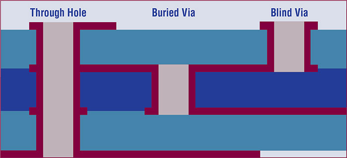
Figure 2. Via types.
Drilled vias. Mechanically drilled via holes are kept small for space concerns and have a special relationship with PCB thickness due to the process by which the holes are plated.
Laser-formed vias. Due to the conical shape of a hole formed by laser while burning through material, pay close attention to the width/depth relationship capabilities of the process. A 1:2 ratio between the width and depth is considered manufacturable.
Selecting the proper via type will not only help complete trace routing, but can also help in alternate applications for uses like EMI shielding and thermal management. However, choosing any via type other than a common through-hole via with a modest hole diameter/board thickness aspect ratio will most certainly incur a cost adder.
As with most things in PCB manufacturing, as via size shrinks or the complexity goes up, the “yield” of the PCB run may go down as some part features, such as vias, fail to pass inspection. Blind and buried vias will incur cost adders because of the unique processes involved.
Vias are often a necessity. Knowing the different types, benefits and potential costs will help toward selecting the best via for your needs, while avoiding cost and manufacturability issues downstream.
Utilizing planes and pours. Power planes are the most effective way to distribute power to almost every part of the PCB. Power planes are simply formed by adding layers of copper foil to the stackup and connecting them to power or ground. Smaller SMT parts located any place on the board surfaces can connect to a plane by use of a via. Larger SMT parts requiring more power can use multiple vias connected to the power planes. By their physical nature, through-hole parts will easily connect to the planes as required. However, for high-current requirements, designers sometimes add support vias around a component pin to increase the current path to the pin.
Besides power distribution, copper planes can be utilized for many other purposes, such as:
- EMI reduction return path
- Added capacitance
- EMI shielding and ESD guard band support
- Thermal management (heat-sinking).
Impedance control and signal integrity. Industries requiring quick digital applications such as telecommunications, video, computing and others rely on impedance control to minimize signal degradation and improve signal integrity. A PCB design engineer needs to recognize controlled impedance requirements on a schematic and manipulate several parts of the design layout to achieve the requirements.
Impedance control on a PCB is required when performance dictates signal degradation in a circuit cannot vary beyond a specified amount, expressed in ohms Ω. Impedance control requirements for PCB layout can be addressed physically in the layout by identifying nets in the design to control by their specific impedance value. Always seek approval from the fabricator after estimating impedance stackup solutions.
Certain circuits require routing parameters that must be held for the device signals to run properly. Signal routing parameters are documented in the component manufacturer’s data sheet. Several parameters must be noted when performing placement of the chip, its related components, and when completing the routing. These include:
- Lengths and routing order of critical signals to match to related signals
- Hub routing constraints where a signal routes to a given point and then splits off to several length-matched destinations
- Distance to adjacent signals could permit unwanted signal coupling or crosstalk
- Impedance control, either single-ended or differential
- Unbroken reference plane running beneath signal routing layers.
Sometimes PCB electrical performance considerations conflict with manufacturing considerations. A designer must be able to quickly assess the appropriate compromise between the two. Often companies will have an SI expert or consultant who specializes in these types of high-speed signals to ensure proper operation. While every designer may not be an SI expert, having a solid understanding of the critical signals and the general requirements needed to ensure acceptable signal integrity will help minimize issues found by the SI expert or in test.
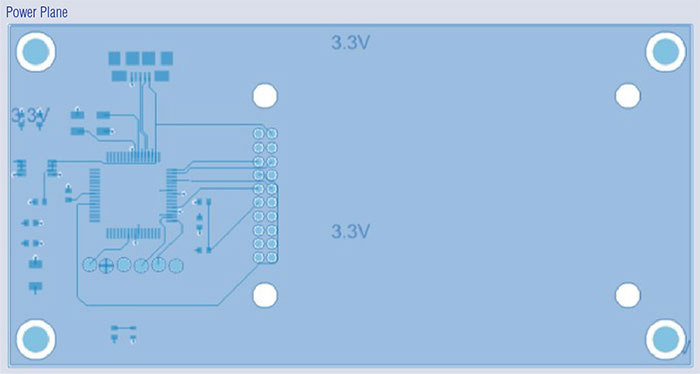
Figure 3. Power plane.
Routing. Routing is a highly subjective topic due to the myriad constraints that may be present within the design. A designer must not only get a layout routed, but the design must perform electrically. Subjectivity aside, a few considerations must be implemented in the interest of both electrical performance and DfM. These include:
- Fanout
- Routing power
- Routing critical lines.
There is a saying in the PCB design industry that “90% of the routing on a PCB takes only 10% of the time, while 10% of the remaining routing can take 90% of the time.” This perspective describes a designer’s experience toward the completion of a layout when the fun of routing turns into an ever-increasing challenge. Suddenly there is a realization all the fun routes have eaten up all the routing space. The routing challenge will most certainly turn into defeat and a complete do-over if the remaining 10% of the routing includes any critical signals. Keep routing fun and challenging. Consider critical net noise, clearance, and establishing shortest routing paths first. At the same time, consider avoiding adjacent layer parallelism and eliminating circuitous routing paths. Avoid complete routing do-overs by routing critical lines first.
It might be easy for those who do not understand PCB layout to sum up the process as simply “fitting the parts on the board and hooking them together.” The intent here is to give a new designer basic routing points to consider before, or instead of, simply activating an autorouting routine.
Successful routing and plane utilization have a direct effect on circuit performance. Implementing setup, routing and establishing copper planes in a PCB layout can make the difference between a dot-to-dot hookup technician and a designer. Metaphorically, this comparison may be likened to the steps a skilled photographer would implement to create a classic photograph. Without understanding how to properly set up and manipulate the subject matter, lighting and exposure controls, a camera operated by the click of novice may only yield a cheesy snapshot.
This excerpt of The Hitchhiker's Guide to PCB Design was written by EMA Design Automation. Download to learn more about PCB design stakeholders and real-world, actionable PCB design tips from industry experts (go.ema-eda.com/pcbguide).


