 Should you use wider trace widths? And how will you know?
An engineer recently asked me about the relationship between trace width and insertion loss, while adjusting dielectric height to maintain a 50Ω single-ended impedance.
At a high level, five variables are at work here, including trace width, copper weight, dielectric height, Dk and Df. Include frequency and resin content, and we’re really talking about seven variables. (Then there are stripline vs. microstrip configurations, which change things a bit, as well as percent-copper, which impacts prepreg thickness, and copper roughness.) We’ll keep things simple, for discussion’s sake, and address some of these factors in future columns.
Lossy transmission-line effects become significant signal integrity concerns at clock frequencies above roughly 1GHz and for interconnect lengths that exceed 12 inches. Assuming we’re talking striplines and grabbing data from a stackup I was looking at [Megtron 6 (G)], we’ll use an insertion-loss comparison between two different trace width/dielectric height combinations. (Dks are similar, but a little bit different, depending on resin content.)
Example design. From Megtron 6 (G) tables, an example 8-layer stackup provides a convenient illustration:
- Layer 3 — Narrow trace width, thinner dielectrics
Width = 3 mils
Cores at 3 mils (single-ply 1078 glass); half-oz. copper
Pressed prepregs at 2.64 mils (single-ply)
- Layer 6 — Wider trace, thicker dielectrics
Width = 5.5 mils
Cores at 5 mils (dual-ply 1078 glass); half-oz. copper
Pressed prepregs at 5.64 mils (dual-ply 1078 glass)
- Electrical characteristics for dielectrics:
Cores: Dk = 3.64 (RC = 54%); Df = 0.004
Prepregs: Dk = 3.4 (RC = 63%; 1078 glass); Df = 0.003
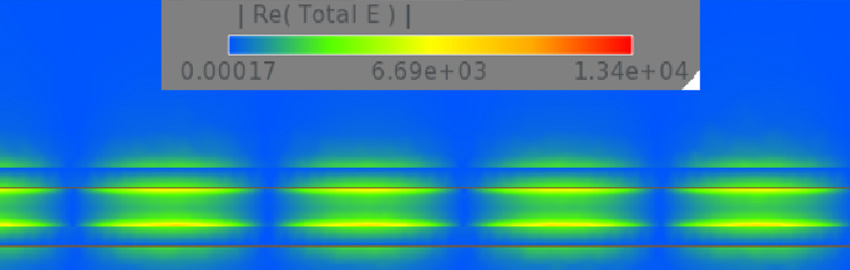
At 4GHz, column Y in FIGURE 1 shows insertion loss computed at 0.44dB/in. for the 3-mil wide trace on layer 3 and 0.29dB/in. for the 5.5-mil line on layer 6, in accordance with the conventional wisdom that a narrower trace width results in increased signal attenuation.
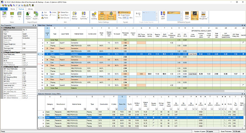
Figure 1. An 8-layer example stackup using Z-planner software shows a 3-mil wide trace width on layer 3 and a 6-mil trace width on layer 6, with both single-ended impedances at approximately 50Ω.
Key loss components. Beyond copper-roughness considerations – a topic for a future column – there are two primary components of insertion loss: conductor loss and dielectric loss.
Conductor loss: From DC through frequencies up to a few MHz, the current in a trace moves through the entire cross-sectional area of the trace. At higher frequencies, however, current flows along the perimeter of a line, rather than uniformly across the entire cross-section. As a result, the series resistance of the signal and return path conductors increases with the square root of frequency as the effective cross-section of the interconnect path is reduced. This type of loss is often referred to as “skin effect.” With any name, it’s something to be concerned about at 1GHz and above.
Dielectric loss: The second important loss mechanism is dielectric loss, which is simply the conversion of electrical energy from the alternating electric field into heat. Dielectric loss is often specified in decibels per inch, increases with frequency, and varies inversely with a material’s dissipation factor, or Df, which is a function of the material’s resin type and molecular structure. Depending on resin content, “standard loss” FR-4 materials have Dfs ranging from 0.015-0.02. Lower Df values equate to more of the output signal getting to its destination, as well as higher material costs, compared to standard-loss materials.
Since we used similar dielectrics on both signal layers in our example, we shouldn’t expect the dielectric loss component to be much different between the narrow trace on layer 3 and the wider trace on layer 6. We can confirm this by using software tools to examine the contributions of conductor loss and dielectric loss for these layers. Layer 3 results for the W = 3 mil case are shown in FIGURE 2.
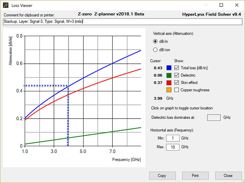
Figure 2. The loss viewer shows a breakdown of the contributions of dielectric loss (0.06 dB/in.) and conductor loss (skin effect; 0.37 dB/in.) for layer 3.
Here we can see dielectric loss is only contributing 0.06dB/in., while conductor loss (skin effect) is contributing a full 0.37dB/in. – a full six times the dielectric-loss contribution! Of course, we would want to multiply insertion-loss numbers by trace lengths to produce total channel losses.
FIGURE 3 shows the same plot for the 5.5-mil trace on layer 6. Here we can see that our dielectric loss hasn’t changed, while skin effect has dropped significantly – to just 0.23dB/in. Of course, the thicker dielectrics would result in a bigger overall board thickness, but if you’re hunting for eliminating the last few decibels from an interconnect budget, it’s helpful to have gained this insight early in the design process.
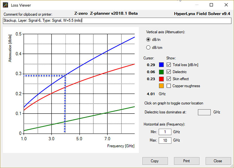
Figure 3. The loss viewer shows the relative contributions of dielectric loss (0.06 dB/in.) and conductor loss (skin effect; 0.29 dB/in.) for layer 6.
Conclusions
We could go a good bit further with this example, looking at higher-loss but lower-priced laminates. We could also explore the effect of copper roughness and resin content. We’ll look at some of these additional design factors in a future column.
Some say trace width isn’t a big deal when it comes to loss, but here we learned wider trace widths can be a great lever for reducing insertion loss. Megtron 6 (G), a relatively expensive low-loss dielectric, under-represents the range of dielectric-loss possibilities among the various laminates on the market. For an actual design, you may want to make material tradeoffs in a stackup design tool, and then specifically discuss the tradeoffs with your board vendor.
Bill Hargin has more than 20 years’ experience in PCB design software and materials. He is director of everything at Z-zero (z-zero.com); This email address is being protected from spambots. You need JavaScript enabled to view it..