With few exceptions, large vias are not ideal for ground pads.
I recently received a question on Twitter, asking: “What is your opinion on the ‘one big plated drill in QFN ground pad’ pattern?”
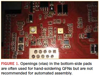
I answered back in 140 characters or less: “Bad for machine assembly, okay for hand assembly.” That’s definitely a true statement, but it’s worthy of a bit more explanation. Figure 1 shows the side opposite of where the QFNs are mounted. The two big openings in the square gold pads are the big vias (plated drill). This is often done when hand soldering QFNs. First, on the component side, solder the little pins on the outside edge of the QFN. Then turn the board over. Stick your soldering iron and solder into the big opening to solder the pad down.
Generally, there wouldn’t be any reason to do this with machine assembly, as we do here in our plant. The proper thermal approach is to put a number of small capped vias in the pad area. The solder paste layer (AKA stencil layer) in the CAD library needs to be segmented to allow for 50 – 75% paste coverage. Thus, we would never recommend using big vias, like those in Figure 1, for machine assembly.
However, I can envision some situations that might call for this. First, when hand soldering, as I mentioned above. Next, there may be some very specific need to expose a lot of the pad to open air for cooling. This is not the best way to get cooling, but it may work in some special instances. Third, perhaps access is needed to the pad as a test point and there’s not enough room to get access any other way.
None of those three steps would be taken in a production environment, but in a prototype world sometimes things happen differently.
SMT? Or not? Sometimes parts labeled as surface mount aren’t quite ready for prime time. In this case, I’m not referring to components that aren’t up to thermal par. Instead, I’m talking about components that can take the heat, but aren’t set up to be machine assembled.
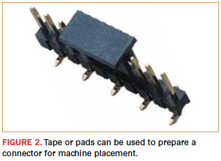
Surface mount machines need a flat surface to pick on. The machines use small vacuum nozzles that need to seat on that flat spot. Chips, of course, are flat on top, as are most other components. Connectors, however, are often not flat on top. That doesn’t leave any place for the pick-and-place machine to pick.
Generally, manufacturers will place a small tab of Kapton tape or a small snap-in plastic pad on top of the connector, giving the machine a surface to work with (Figure 2). Once the board has been fully assembled, the tape or plastic pad is simply removed.
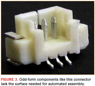
Every now and then, we’ll see connectors come in without that flat pick-and-place surface (Figure 3). That means the machine can’t place it, so it will have to be placed by hand. If there’s a choice between a part with the tape and one without, pick the one with the tape. No offense intended to all of you humans, but machine assembly is way better than human assembly.
Duane Benson is marketing manager at Screaming Circuits (screamingcircuits.com); This email address is being protected from spambots. You need JavaScript enabled to view it.. His Twitter handle is @pcbassembly.