Grounding and routing tips for sensitive parts.
Years ago, I set out to become a world-famous PCB designer. The journey, however, took much longer than that. Starting near the beginning, the second lesson I learned about electronics came on the first day on the job in electronics. I bet you’re wondering what I did in electronics on my first day.
My contribution was to put completed printed circuit board assemblies into pink bubble wrap bags. The bags were sealed with resealable ESD warning stickers and placed in individual boxes. Labels on the boxes had blanks for the information, which was copied from the board to the label. Completed sets of eight boxed boards were again boxed in a larger box, which was labeled with the content part numbers, revisions and so on.
As an aside, the next stop for the boxes was the shipping department and, finally, phone company offices around the country. Called offices, they were more of a precursor to today’s data centers. The build-out was a result of the US government forcing the phone company to break itself into regional businesses.
What our equipment did was allow 384 voice calls on T1 cable originally built out to carry 24 such lines. The T1 interface was one of the more interesting looking cards, with a lot of passive parts. Whether it was a modulator/demodulator board, or the more expensive A to D converter and so on, they all had pink bags and orange stickers as part of their final prep.
By now, you’ve guessed that the second lesson I learned was about electrostatic discharge (ESD). We had to watch a film and tolerate constant reminders to plug our wrist straps into the bench before we began work. Larger areas where the equipment racks went together had special floor mats and shoe straps. Earth ground was achieved with an actual stake in the concrete floor to create a common point ground. It was a normal function to prepare the workspace before working on static-sensitive products.
One of the tenets of the system was regular verification of compliance with the established ESD processes. Auditors could show up at any time with their clipboards and checklists as part of ISO certification. Having a certified factory is one thing. The driving cause was to reduce scrap and its erosive effect on business results. Profit matters. No matter who you were, you needed a smock and proper awareness to go into the ESD-safe zones.
It was the time of very large-scale integration. VLSI was the buzz phrase that implied hundreds of thousands of transistors on a single die. The six-digit number of gates is now a nine- or ten-digit number that takes about the same amount of space. Integrated circuit geometry has been reduced by orders of magnitude, to the point of vanishing entirely.
Seriously, our eyes can only work with visible light that comes in wavelengths between 380 and 700nm. The geometry of early microcontrollers and microprocessors wasn’t even measured in nanometers, as we see on today’s devices. “Deep sub-micron” only hinted at what was to come. Generation after generation, the tiny features have always required protection. Electrostatic discharge is the same threat today.
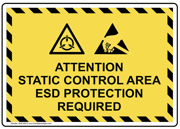
Figure 1. Two different symbols indicate ESD zones, with the hand being the more common. (Source: Compliance Signs)
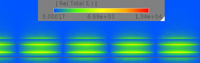
Cause and effect: magnetism from an arc. Random high-voltage spikes generate rapid change in the electromagnetic fields. The system sees that as a huge noise spike, in addition to the potential damage done by the voltage. Reactance is the natural byproduct, and it has a wider reach than the tiny arc of electricity that sets it in motion. The good news is we have a few tools to keep our electronics safe.
- Ground the connector’s body to a perimeter seal ring that creates a Faraday cage around the PCB edge. This might be a partially isolated ground, depending on the circuit.
- The transient suppression circuit is helped by localized mounting holes where the PCB ground is tied to the enclosure. Anchoring the connector is good for mechanical reasons, too.
- Place ESD diodes near the connector (ESD source) and route with short, unbending traces, including a low-impedance ground termination. Multiple ground stitching vias are good, if there is room for such things.
- You don’t necessarily want sensitive components to be placed near the connector/ESD diode region. A little routing will do some good, up to a point.
- These additional ESD suppression components will eat into your loss budget, so try to maintain low capacitance on the signal going down the line.
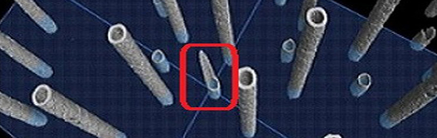
Figure 2. Swaged turret terminals such as these provide a high-reliability method of connecting wires to a PCB. We can’t rely on the strength of the copper barrel of the plated hole. (Source: Greenhouse Lighting)
Going beyond the layout considerations, the particular assembly process documentation and general workmanship manual should stress the importance of proper PCB handling with respect to ESD. Those documents would be called out by reference on the assembly drawing.
Some manufacturing engineers will request we add notes to the assembly drawing that detail some or all the processes of the assembly. Lab coats and straps have nothing to do with the state of the product when it is all done. They are a means to an end. The assembly drawing is not a how-to but rather a what-is type of document.
The wisest course to bring ESD awareness to the assembly and test benches is to label the board accordingly. The marking on the board itself should indicate it has sensitive components as the largest single piece of information. The purchase order should include packing instructions for safe transportation.
Taking an interest in electrostatic discharge shows that you care about the bottom line. Being mindful in the lab or wherever electronic components are exposed will help those parts reach their full potential as part of a working unit. Make it happen. •
John Burkhert Jr. is a career PCB designer experienced in military, telecom, consumer hardware and, lately, the automotive industry. Originally, he was an RF specialist but is compelled to flip the bit now and then to fill the need for high-speed digital design. He enjoys playing bass and racing bikes when he’s not writing about or performing PCB layout. His column is produced by Cadence Design Systems and runs monthly.
PCB West: The leading technical conference and exhibition for electronics engineers. Coming Oct. 4-7 to the Santa Clara (CA) Convention Center. pcbwest.com