An experienced engineer takes their first trip to a board shop.
Time was, PCB fabrication was a standard in-house function of OEMs. IBM, Digital Equipment, AT&T, Texas Instruments, Rockwell and hosts of other large and not-so-large OEMs had captive operations. Board “design” meant place and route, and was a specialty, as was library management and engineering.
Today, of course, that’s all changed. As specialization on one end has ended, it’s become the norm on the other. Fabrication is largely a merchant exercise. And a designer does a little bit – or a lot – of everything.
What’s been lost on the way is the knowledge of how a board is made. No longer can designers take the long walk from one end of the campus to the other to witness the process and talk to the operators and process engineers in person. Communication now ends at the CAM station, if it even makes it there. A surprisingly large contingent of designers today have never seen the inside of a board shop, let alone had the opportunity to get their questions answered.
What, PCD&F wondered, would a board shop look like through a first-timer’s eyes? We had the opportunity to find out in late July, when we accompanied one such person on his first trip through a plant.
Joe Labonte is by all metrics an industry veteran. He’s been involved with OEMs in the industrial instrumentation sector nearly four decades. Some of these large- and mid-sized companies had fabs, but none were local to his site. He’s visited many EMS companies and is the engineering interface for the one used by his current employer, an international OEM of industrial water treatment control systems. He has done some designs and still handles parts of the PCB design process, although most of his career has been spent as the interface among electrical engineers, experienced PCB designers, PCB fabricators, and contract assemblers. But before July, he’d never stepped foot inside a fab plant.
The first thing Labonte noticed – as is typical with most who walk a board shop – was the odor. It was familiar to him, but he couldn’t quite place it. That scent was the ammonia that is part of the etching chemistry. To the uninitiated, it can be strong. Over time, while it remains noticeable, it becomes part of the background, like gasoline at a filling station.
Circuit Connect operates a 27,000 sq. ft. site in Nashua, NH. Years ago, the area was hopping with major fabricators. Hadco (and later Sanmina) operated multiple plants in and around Salem. Fifteen miles away, Teradyne operated perhaps the most technologically proficient board shop in North America. Even closer was Parlex’s primary flex circuit plant and international headquarters.
Today, like most of the US, volume production has disappeared. In the heydays of the domestic PCB market, Circuit Connect would give away prototypes in order to attract future volume orders. But the volume stopped materializing. It went through a fundamental transition in the mid-2000s, shifting from a volume plant to one that makes its living in the high-mix/low-volume space. The company now employs 35 to 50 staff, depending on the season, including four engineers. It holds 10 certifications and registrations, including ISO 9001 and 14001, ITAR and UL.
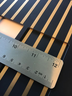
Figure 1. A “sculpted” PCB made for Teradyne.
Our hosts included CEO and owner Rick Clutz Jr. and president Bob Lazzara. Clutz is an industry lifer, having previously run CuTronics in Baltimore. He purchased CuTronics’ Nashua plant in 1990, forming what became Circuit Connect. He then acquired Time Sensitive Circuits in 2010, which was rolled up into the Nashua plant.
Common Background
Perhaps more than anyone, Lazzara could relate to Labonte. Lazzara started his career in electronics not in fabrication but as a designer with Bell Labs/Western Electric, at which he worked nearly 20 years. He joined Circuit Connect in 1995 and became president in 2014.
US shops have become adept and creative, and Circuit Connect is no exception. Its typical product is two to 12-layer boards with lines/spaces down to 3/3. Boards will have standard copper plating, or up to 10 oz. with 5/5 lines/spaces. Circuit Connect can build up to 42 layers in production. On a given day, it will produce about 150 panels.
Circuit Connect also makes non-PCB products. Examples we saw included a 0.320" heavy copper product with solder mark and gold edge plating used for motors (FIGURE 2), and a 10-layer (with 3 oz. copper per layer) submersible pump. A third product was a 38-layer solid state rectifier (FIGURE 3), which is built for Boulder Wind and is used in wind farm generators in the North Sea.
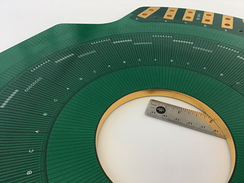
Figure 2. Circuit Connect applies its PCB knowledge to non-PCB products, such as this 0.320" heavy copper product with solder mark and gold edge plating …
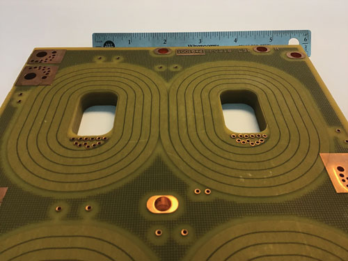
Figure 3. … And this 38-layer solid state rectifier (solder mask removed).
Circuit Connect’s engineers resolved a problem for a power semiconductor manufacturer in which the glue for the heat sink was failing, and the chip would fail. Some material vendors had epoxies that could handle the conductive or adhesion functions but not both. Circuit Connect helped devise a design that shored up the device.
A more assertive example of its engineering prowess was a military weapon in its conference room, in which Circuit Connect machines wells (pockets) in the FR-4 to add a connector-less flex. (Taiyo makes a non-glossy solder mask just for this product.)
“Our core business will always be the fabrication of bare, ready-to-assemble PCBs,” explains Lazzara. “We can build one PCB and give you a plan for how we can build 10,000. However, Circuit Connect is surviving offshoring by augmenting our core PCB business with the manufacture of non-traditional PCB products. These are designs that combine PCB materials and methods of manufacturing for end-products that are not PCBs.
“This is a growing market in want of a name. With these quasi-PCBs, the novelty starts with the materials and methods of manufacturing before leading to very novel – some would say revolutionary – end-products. IP is of equal or greater importance today” for the US domestic market, he adds.
Processing materials is, of course, what fabricators do. Yet, as Lazzara notes, “Decisions aren’t always based on experience. Designers often lack materials knowledge. They sometimes rubber-stamp things on prints.”
Targeted Automation
Circuit Connect uses FR-4 and polyimide, including a range of thin high-frequency materials. It competes with other fabricators through targeted automation and avoiding material waste.
“PCB fabricators in North America used to be able to sell technology or time,” he notes. “They still can, but look at the cellphone PCBs. It’s almost impossible to compete on that.”
To that end, Circuit Connect explained its transition to digital imaging. Labonte asked about the multiple operations the digital imager performed, seemingly new to that technology. Lazzara showed an RF panel built for a prime defense contractor (FIGURE 4). The panel was seven-up, a switch from a previous design in which each board was purchased individually. That meant seven unique board processes and seven solder paste stencils. Now, Lazzara noted, the panel requires a single setup and just one solder paste stencil. Although the re-spin means the entire board is done in gold and with Rogers material, the final panel is less expensive, even at the PCB level, because it consolidated the board processes. As a bonus, Circuit Connect found the new design tuned better, which improved first-pass yield at test. It also simplified paperwork because it reduced the RoHS declarations, certificates of conformance (C of Cs) and first article reports again from seven to one.
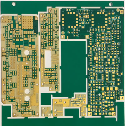
Figure 4. A five-up RF panel built on Rogers material.
Circuit Connect uses a standard panel size of 18 x 24", and squeezes as many boards as possible into each one. It offers a fixed price for two, four or six layers. And while it mixes different layers on the same pallet, it does not build multiple customers’ part numbers on the same panel.
“So, you take several different design outputs and quote it?” asked Labonte.
Lazzara: “We do. We try to bring all those elements together. It may not work on everything, but where it does, it saves money” (FIGURE 5).
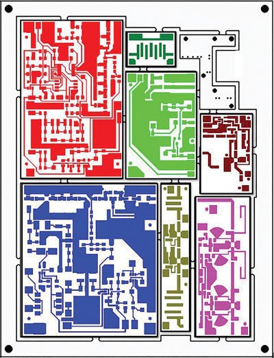
Figure 5. An actual eight-unit layout proposed to a client during quote.
Labonte appeared impressed. His company’s typical board design is two to eight layers, with 4/4 lines/spaces. (Its supplier, although US-based, is not Circuit Connect.)
A tour of the factory proved equally informative. We walked the plant in somewhat the same way the design travels from the OEM to finished goods. Most CAD files Circuit Connect receives are in Gerber 274X format, as they prefer. They use Frontline Genesis and Numerical Innovations for CAM.
One interesting development, unexpected for a shop this size, was Circuit Connect’s investment in its own DI water system. The company is working with New Hampshire state regulators toward a zero-discharge system, which is driven by personal goals, not regulation, Clutz explained.
Labonte wanted to know Circuit Connect controls surface cleanliness. His company is “drifting back” toward cleaning, he added. “At the customer’s request, we use a DI water rinse and check with a contamination checker,” Clutz said.
Two Maskless Lithography LED direct imagers were present for solder mark and outerlayer imaging, the second having been installed in late 2018 (FIGURE 6). With the additional machines, Circuit Connect was able to reduce its head count while increasing its output. Now, one operator runs both machines. The direct image solder mask can yield 3-mil dams.
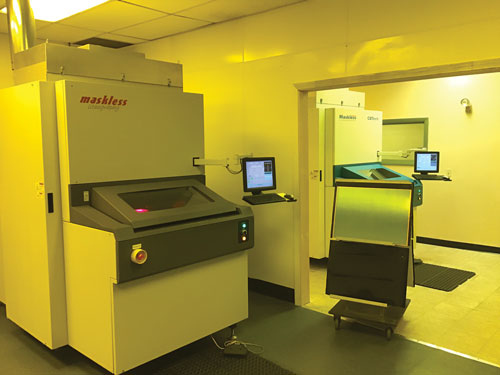
Figure 6. Recent investments include Maskless Lithography LED direct imagers for solder mark and outerlayer imaging.
The two developers have a capacity of 600 panels/day. The batch copper electroplater includes acid and alkaline systems. We spent a moment discussing the differences between vertical and horizontal plating. Less elaboration was on the graphite line, which works by chemically bonding a layer of graphite to the hole wall and is used in place of electroless copper.
The plating lines were typical: copper, tin, nickel, gold. Circuit Connect also has a Teledyne Halco 175 horizontal Pb-free hot air leveling line, and offers ENIG, immersion silver and hard gold finishes.
Clutz indicated that Circuit Connect sees silver as the most-economical lead-free finish today. Labonte allowed that his current company underwent a thorough assessment of finishes during its RoHS conversion, settling on ENIG as the best and most cost-effective method.
At lamination, Burkle hot and cold presses are used. Labonte wanted to know how much time product spends in lamination each day. (Answer: two to three hours.)
Circuit Connect has three mechanical drills: an Excellon Century 2001 six-head drill, a Mark VI five-head drill and an Excellon five-head drill, plus Excellon routers. The question was raised about laser drilling and why it would be used. Circuit Connect cannot justify the cost of a laser, given the speed and hole sizes it currently needs. However, an x-ray drill is under consideration for tight stackups, as it can readily locate targets within the copper of innerlayers. Labonte also wanted to know how many layers are stacked on a drill. The answer is it varies, based on the thickness of the materials.
Testing is a big part of Circuit Connect’s protocols. As Clutz said, “I believe in testing everything.” It features a CIMS (formerly Camtek) AOI with 2-D metrology, plus four testers, including a CL Tech Precise FP8 four-head flying probe, and ATG A5NEO eight-head flying probe, the latter of which was installed this year. There are multiple automated cross-sectional analysis machines. Other services include advanced analytical tools, for instance scanning electron microscope (SEM), which is uncommon for the region’s board shops.
Circuit Connect goes beyond traditional PCB fabrication. What it does is fundamental – lamination, plating, etching, testing – but the broad range of its end-products, processing strategies, and investment priorities makes it atypical. Indeed, there might not be a “typical” US board shop anymore.
Still, Labonte was enthusiastic about the day, and PCD&F was thrilled to join him. “I really got a lot out of it,” he told me. Designers, take note and don’t be shy about reaching out to your local fabricators.
Mike Buetow is editor in chief of PCD&F/CIRCUITS ASSEMBLY; This email address is being protected from spambots. You need JavaScript enabled to view it..


