How to Produce an ECO or Update an Existing Design
Changing a part may be simple, but making dozens of edits to a schematic requires a clean process.
With the CAD tools available today, it is a relatively simple process to create a schematic and pass the netlist or connectivity information to the PCB layout portion of the CAD software and create a printed circuit board layout.
Most CAD designers get the layout correct the first time and never make layout changes after board files go to production. For the purpose of this article, let’s call this Revision 0 (Rev 0).
For those who do make errors, they are usually minor, and we make those changes through a process change or engineering change order (ECO). Some companies may use the term document change order (DCO), but for the purpose of this article we will refer to this process as ECO.
Sometimes an engineering group will decide to make changes to the Rev 0 design after the initial prototypes are built. Reasons for making changes are varied and may include swapping parts due to pricing and availability, end-of-life (EOL), correcting errors in the schematic or PCB layout, and so on.
In such cases, changes are made to the schematic; the revision of the schematic is bumped to Rev. 1, and a new netlist is generated. The netlist is then imported into the existing PCB layout, which is also bumped to Rev 1; the changes are merged into the PCB, and the resulting updated files are generated and submitted to production.
Let’s say the changes involve altering values of parts, such as a resistor from 1kΩ to 100Ω, or a capacitor from 0.1µF to 0.01µF (FIGURE 1), and the land patterns or footprints remain the same. In this case, the process involves only changing the schematic symbol, while the footprint for the PCB remains the same. When the schematic gets recompiled, the new information gets passed to PCB layout. In this case, there are no issues when performing the ECO process. The changes are imported into the PCB layout, and new design files can be created.
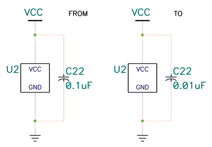
Figure 1. When part values are changed, but not the footprint, only the schematic symbols are modified.
If the engineer deletes parts from the schematic (such as C21 and R15), and then later adds new parts to the schematic, the CAD software will add the new parts to the schematic using the next available reference designators, which might be C21 and R15. This is an automated process that the CAD software uses to try to prevent “holes” in the reference designators used on the schematic and PCB layout.
When the netlist or ECO is created within the schematic capture portion of the CAD software, and is pushed forward (imported) to the PCB layout portion of the CAD software, it sees C21 and R15 already exist on the printed circuit board, so only changes the part values and/or the footprint to the new values to match the schematic. That fulfills the intent of the ECO process built into the CAD software. It does not first delete the footprints from the PCB, and then add them to the board like new parts, around the outside edge, ready to be placed on the PCB. This is what we intended, and what we want to occur. Since the board is already routed per Rev. 0, this causes design rule check (DRC) errors, and the designer is left with the task of deleting and updating the traces and parts and revising the PCB layout manually (also known as clean-up) to correct it to match the new Rev 1 data that now make up the current design. The other scenario is the CAD software will automatically remove any traces it sees as being incorrectly routed, leaving the design with parts on the board with no traces.
While it may not be difficult to update the design if only one or two parts are changed in the schematic, it can be quite a challenge if the schematic has 20 or more changes that affect the PCB.
The process of clean-up may add hours or even days of unnecessary time to the PCB layout. That means added cost and a possible delay in the completion of the revised design and the release of new CAD data to production for Rev 1 boards. This also means a delay in the overall delivery schedule of the finished product. All this is due to a “simple” change to the original CAD design that was incorporated by way of the ECO process.
A Better Method
What is the correct (or better) method to use for implementing the ECO, so the engineer and designer can coordinate efforts to create an updated schematic and PCB layout with minimal disruption to the existing design and schedules?
To work within the processes built into the CAD software, take the following steps:
Before updating or making any changes to the schematic that involve deleting components and adding new ones, the engineer (or individual responsible for making changes to the schematic) needs to create or generate a “Last Component Used” list. This list documents the highest reference designators (RefDes(es)) used in the schematic. For example, R57, C35, U13, etc., might be the last components used in the above example. When the engineer proceeds to make changes, such as deleting C21 and R15 as in our example, these components and reference designators no longer exist in the design (FIGURE 2). However, when adding a new capacitor, use the next higher reference designator above the highest RefDes used in the design, which would be C36, as in the example. The next resistor added would be R58, and so on (FIGURE 3). The deleted RefDes(es) of C21 and R15 are to be considered dead and will be “holes” in the list of RefDes(es) that get passed to PCB layout. If there are already holes in the RefDes(es), they should be ignored, and the process should follow using the reference designators above the ones listed in the Last Component Used table.
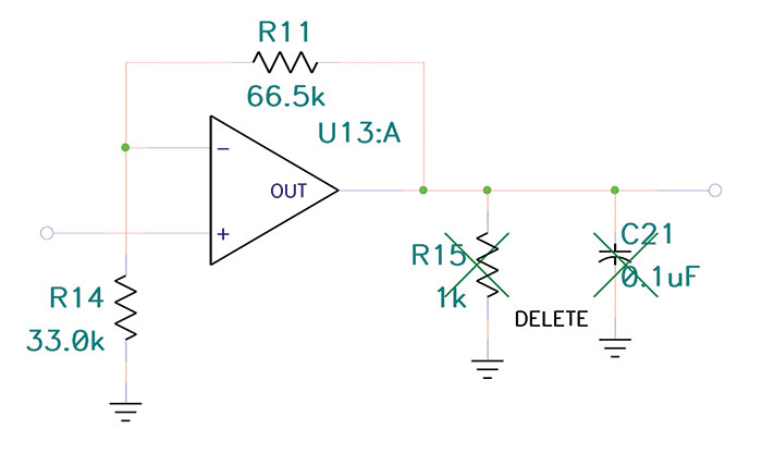
Figure 2. Changes to parts eliminate the components and reference designators from the design.
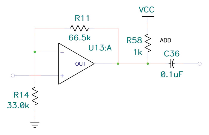
Figure 3. Newly added parts are assigned the next higher reference designator above the highest RefDes already used in the design.
To implement this process, the engineer will need to physically change the RefDes after it is placed in the schematic. The CAD software will place it and name it C21 or R15, as in our example. The engineer will then need to attribute the part and change or override the RefDes(es) and change them manually to be the new RefDes(es). This may take some time but is necessary for the process to work cleanly.
When the ECO or new netlist is generated, there is no conflict with existing RefDes(es) on the PCB layout. If an ECO is used to pass changes to the new PCB layout, the C21 and R15 parts will be deleted from the printed circuit board, and the new C36 and R58 will be added to the design, and most likely placed around the outside edge of the board outline. These newly added components are now ready to be moved onto the board and placed in their proper locations with a rat’s nest to their connections on the board.
The PCB designer can then remove any dead traces connecting the deleted parts C21 and R15, proceed to move and place the newly added C36 and R58 onto the board, and route traces to them, to complete the update of Rev 1.
Of course, to eliminate the holes left by deleting the components in the schematic (C21 and R15 in our example), the CAD designer will need to perform a RefDes renumber on the board, and then back-annotate this information to the schematic, which will keep the PCB and schematic in sync.
In either case, a list of any and all deletions, additions or changes to the parts on the schematic needs to be documented and used in any company-related ECO, which will affect the bill of materials (BoM) and production.
In conclusion, to properly update a printed circuit board with minimal work, the engineer and CAD designer need to work in harmony to update an existing design, while utilizing the aforementioned information.
, is president at Oztronics (oztronics.biz), a design service bureau; This email address is being protected from spambots. You need JavaScript enabled to view it..


