Smaller part sizes require less solder and can eliminate parasitic inductance.
Even after decades of downsizing, passive components still take up approximately 70% of board space, making continued miniaturization a primary design concern. However, the pace at which miniature technology is adopted is dependent on how quickly manufacturers can reduce the cost of this process. With regard to passive components, the essence of both downsizing and reduced costs is volumetric efficiency.
A common but overly simplistic approach to achieving capacitor cost savings is to shrink the size of a component for a given capacitance and voltage rating in hopes that the resultant material reduction will instantly diminish costs. However, material cost is only one factor of the total cost of component manufacturing. The R&D and process development costs required to achieve material downsizing often outweigh the gains, especially at the front-end of introduction. These costs diminish as the process matures, eventually enabling overall component cost savings, but results are far from immediate.
Any adequate examination of the evolution of capacitor downsizing needs to consider their construction. Although multilayer ceramic capacitors (MLCCs) and tantalum capacitors have progressed along a similar path with regard to miniaturization, their different materials and constructions contribute to a few notable evolutionary variances.
Surface-mountable MLCCs are straightforward devices that store a charge between pairs of electrodes, which are often stacked. The resultant capacitance is enhanced by an insulating ceramic dielectric material placed both between the plates and around the active portion of the device. MLCCs are manufactured by layering a base plate with several sheets of ceramic dielectric material in its “green”/unfired state, up to several hundred additional layers of dielectric material each screen-printed with an electrode pattern using metal ink, and another few layers of green ceramic dielectric sheets. The resultant plates – comprised of a green substrate with embedded layers of metallic material patterned into thousands of capacitor elements – are then diced into individual elements, fired and terminated at the ends.
Although the ceramic material is homogenous throughout an MLCC, there are active and inactive areas, both of which must be reduced to achieve further miniaturization. The cover layers and end margins pictured in FIGURES 1 and 2, which act as the insulating case for the part, are the inactive elements of an MLCC. The active, internal areas, where the electrodes overlap, act as a dielectric and store charge.

Figure 1. An exploded view of a single multilayer ceramic capacitor (MLCC).
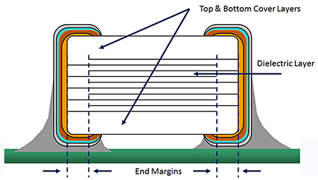
Figure 2. A cross-section of an MLCC reveals the active and inactive areas.
MLCCs require a minimum amount of inactive casing to protect the active region and permit handling. However, this limit can be approached if both the registration of electrode patterns during laydown and the subsequent post-firing dicing operation are executed with great precision. Unfortunately, though, this limit is essentially a constant for all case sizes at any point in time, which means that inactive volume takes up a larger portion of the package as case size is reduced.
In the basic capacitor equation pictured in Equation 1, which allows us to consider the active volume of an MLCC, the capacitance is a function of electrode area (A), electrode spacing or dielectric thickness (d), and dielectric constant (K). So, for a given case size with predetermined margins, the electrode area is set, leaving dielectric constant and electrode spacing as the two variable parameters.
 (Eq. 1)
R&D engineers are continuously trying to improve ceramic dielectric formulations to increase K values and exhibit greater breakdown voltage characteristics over time, the combination of which enables higher capacitance and higher voltage ratings in a given package, but achievements in this regard occur in small, evolutionary steps. The revolutionary aspect of ceramic downsizing in recent years – lower IC core voltages – was application-driven, as handheld and consumer product manufacturers demanded high volumes of significantly smaller capacitors with a narrower operating temperature range than those intended for use in industrial systems.
When calculating application reliability for ceramic capacitors, temperature is a more significant accelerator than voltage, so the ability to formulate materials specifically designed for applications with maximum operating temperatures of 85°C that exhibit higher K than materials capable of 125°C maximum temperature is also a major factor for downsizing.
Tying this in with advances in manufacturing technology, such as improved registration for electrode laydown and improved margin alignment, has enabled major advances with respect to capacitor volumetric efficiency. For example, MLCCs designed for emerging applications that require lower voltage cores (1.8V–3.3V) can use thinner dielectric layers than are required for 4V–6V ratings. Traditional dielectric laydown methods (using green tape processes) had minimum thicknesses corresponding to 10V ratings or above, but more recent methods of slurry deposition have enabled the development of thinner dielectric layers, the significance of which is that (as supported by Equation 1), if the distance between the electrodes is halved, the capacitance value is doubled, albeit at a lower voltage rating. Additionally, halving the distance between electrodes reduces the previous stack height by 50%, so if the number of layers at this stage is doubled, further doubling of capacitance can be achieved.
These developments have enabled high capacitance ratings, such as X5R 85°C µF/6V in compact 1206 packages and 10µF/6V ratings – previously only available as an X7R 125°C in a 1206 size – in a downsized X5R 0402 size, which is where the cost savings come in.
Dicing a given MLCC plate or substrate into 0402 size parts will supply nearly nine times as many parts as the same plate diced into 1206 size parts. (Note: Material waste accrues with each cut made, which is why cutting a substrate into 0402 sizes does not quite supply nine times the number of parts as if it were cut into 1206 sizes). Consequently, this method of material reduction is the primary driver for suppliers’ R&D investments in manufacturing technology.
Now, it is worth noting that suppliers do not ship the finished parts in bulk. Instead, they ship them in a packaging system compatible with high-speed surface mount assembly, typically tape-and-reel or cassette. Similar to the inactive areas of smaller MLCC packages, the packaging material required to deliver subminiature parts also becomes a higher proportion of the total component cost. Recent packaging developments can deliver smaller case size products on finer pitch and narrower tape, but even that isn’t an ideal solution, as it requires users to invest in high-speed placement equipment capable of handling parts with dimensions akin to grains of sand, in addition to feeders capable of handling higher density packaging. To be fair, though, every introduction of smaller-sized MLCCs requires users to consider a host of new factors at every stage of board production, including PCB footprint designs, reflow profiles, handling techniques, and rework techniques, among several others.
So while the process of downsizing MLCCs follows a standard methodology, it is fair to say that each new subminiature capacitor size introduced to the market has been met with some level of skepticism. For example, at each migration from 0805 to 0603, 0603 to 0402, and 0402 to 0201, scores of users speculated that the limit for volume handling of components had been reached and that the industry had finally reached a stage where migrating to dual or quad capacitors in a given package size would be a more viable path to further downsizing.
Manufacturers rose to the challenge of multiple element arrays, but – with the exception of special applications or those in which board real estate is exceedingly limited – the adoption rate of these solutions for general assembly has been low, as users typically found that their ability to adapt to handling smaller-sized components went faster than expected. Consequently, at a discrete component level, handling 0201 sizes has already given way to 01005 size parts, and 008004 size parts are distinctly visible on the horizon.
Nevertheless, special applications for capacitor arrays are also growing. One advantage of having two elements co-manufactured in the same body is that they can be placed across adjacent lines, but will track identically over time with regard to temperature and applied voltage, which is ideal for frequency control applications. Thus, as the manufacture of miniature wireless systems for handheld devices continues to increase, so does the use of arrays, which are also experiencing downsizing trends (e.g., from 0508 to 0306 sizes with two to four elements). Arrays also provide additional cost benefits during PCB assembly. Their smaller terminations require less solder usage per element, and placement speed and throughput for a four-element device is 75% faster than for the equivalent discrete parts.
Additionally, the development and market introduction of fine copper termination (FCT) MLCCs has also aided component miniaturization. This process, first developed at AVX several years ago, has enabled FCT MLCC designs to utilize an electroless copper process rather than a thick-film copper paste process, providing a much more uniform termination throughout the chip and solving one of the primary process issues associated with miniaturization. This method of applying high-precision terminations to ceramic bodies was originally devised for multiple terminations to reduce inductance at high frequency, but now also delivers a dimensional advantage in the manufacture of ultra-thin components. As component thickness decreases, the termination plating thickness becomes more significant. When designing ultra-thin capacitors to meet a 0.25mm thickness requirement, a standard, plated termination with a 20µm thickness will reduce the available active volume by 8%, while an FCT termination of <9µm will take up less than 4%, which is an important volumetric efficiency consideration in very low profile applications, such as wearable and embedded electronics (FIGURE 3).
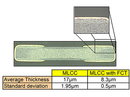
Figure 3. Ultra-thin ceramic MLCC with FCT termination.
Similarly, miniaturization of surface-mount tantalum capacitors – which have traditionally been the main choice for extremely space-constrained devices that require a large bulk capacitance – has progressed in much the same manner, focusing on reducing inactive volume and maximizing capacitance and voltage characteristics for emerging high-current, low-voltage applications. The primary feature limiting the height and package efficiency of tantalum chip capacitors is their conventional molded packaging. In a conventional molded, J-lead package (FIGURE 4), the anode riser wire is welded to one side of the J-lead, while the tantalum element, which features an external cathode coating, is affixed to a lead frame pocket with conductive epoxy. The whole assembly is then molded into a rectangular casing, and the anode and cathode side leads are wrapped around the body to form the external terminations.
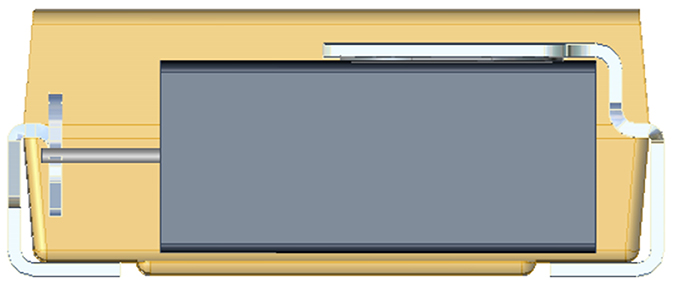
Figure 4. Construction of a conventional molded, J-lead tantalum chip capacitor.
The lead frame, internal anode connection and external molding represent the inactive volume of the device and are akin to the end margins and cover layers in an MLCC package in both function and limitation to miniaturization. Just like MLCCs, as the size of tantalum chip capacitors diminishes, the percentage of its total package volume consumed by the inactive elements increases.
The traditional molded configuration works well down to EIA “A” case sizes (equivalent to MLCC 1206), and even R case sizes (MLCC 0805), but smaller size tantalum chip capacitors require different packaging or construction techniques. As with MLCCs, the problem with scaling conventional tantalum capacitors down to microminiature proportions is twofold: efficiency and manufacturability.
One method of reducing the inactive volume in miniaturized tantalum capacitors is to eliminate the wraparound termination configuration, which can be achieved by internally connecting the lead-frame to the tantalum element and making the anode wire exit the body on the underside of the package instead of extending past the molding (FIGURE 5). In addition to reducing the inactive volume, this facedown configuration also provides an immediate performance advantage. By eliminating the signal loop associated with the wraparound termination, the parasitic inductance of the capacitor is reduced. Moreover, apart from the performance advantage and reduced materials savings affected by the facedown configuration, facedown capacitors require far less solder for PCB assembly and eliminate the need for an external solder fillet, which translates into additional cost savings at the board level. However, the wraparound style is still better suited for larger tantalum packages, as it effectively protects the capacitor from any shock and vibration during mechanical decoupling with the PCB, which is not an issue for small outline molded devices.
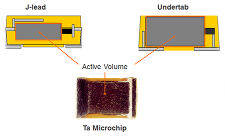
Figure 5. The volume utilization of a traditional J-lead tantalum capacitor as compared to a facedown undertab tantalum capacitor and a high-efficiency tantalum microchip capacitor.
Another method for further overcoming manufacturing and component value limitations – the proprietary TACmicrochip – was developed by AVX and introduced to the market in 2000. The mechanical configuration of tantalum microchip fabrication mirrors that used in parts of the semiconductor world. In this process, capacitive tantalum powder is pressed onto the top surface of a large tantalum carrier, similar in configuration to a silicon wafer, and then sintered in a high vacuum, turning the powder layer into a highly porous tantalum network. Next, the parts on the tantalum carrier are partially cut using diamond cutting wheels to separate the powder layer into a vast array of individual tantalum anode elements. These elements then go through electrochemical processing, which converts them into capacitor elements, are coated in epoxy, and terminated at the ends. Last, the parts undergo a final dicing operation that cuts all the way through the substrate to individualize each component (FIGURE 6).

Figure 6. Structural comparison of a 0805 ultra-thin tantalum capacitor and a 0805 J-lead, facedown tantalum capacitor.
This process has resulted in the manufacture of tantalum microchip capacitors down to the equivalent of MLCC size 0201, which, with miniscule dimensions of 0.6mm (+/-0.12mm) in length and 0.35mm (+/-0.06mm) in width and height, are currently the world’s smallest tantalum chip capacitors. Electrically, these devices exhibit excellent frequency response characteristics, since parasitic inductance is eliminated from the tantalum package. For example, a 0.33µf TACmicrochip capacitor can be built with a tolerance of +/-20% and exhibit less than 35Ω of parasitic resistance (ESR) at 100kHz, a very low value for such a small outline capacitor.
With regard to electrical design, voltages have continued to drop from 5V to 3.3V to 1.5V and below from an application standpoint, which permits the employment of tantalum powder with very high CV/gm (capacitance per unit volume). Similarly, application temperatures for handheld devices are typically far lower than for industrial systems, which typically require a 125°C maximum operating temperature. Although tantalum dielectric is capable of withstanding 125°C, if a design can be optimized with specific de-rating for applications with lower temperature operation, then the capacitance voltage per unit weight (CV/gm) can be increased. In fact, values in excess of 200,000CV/gm have been achieved with this specific tantalum microchip series. Consequently, users have become used to the improving reliability of tantalum capacitors in these low-voltage applications and have begun modifying the traditional 50% de-rating factor to a much more realistic 20% factor in high-impedance circuits.
In sum, miniaturization will continue to be a primary design concern with regard to passive components like capacitors, and the evolution of miniaturization continues to effectively produce significantly smaller parts with higher volumetric efficiency at lower costs than were available even just a few years ago.
Chris Reynolds is technical manager at AVX Corp. (avx.com); This email address is being protected from spambots. You need JavaScript enabled to view it..