Analysis and summary of the most fundamental design guidelines.
Technological advantages associated with the use of laser systems include flexibility, material efficiency and performance. To exploit the potential of filigree laser tools it is necessary to know and understand the physical and technological possibilities and limitations. This article focuses on material efficiency and design rules. Various factors are decisive for the design of PCBs, such as components and their heights, and potential mechanical or thermal stress.
Methodology and Results
The following results are based on experience and know-how collected during dozens of application trials for cutting rigid FR-4 boards in the application department at LPKF Laser & Electronics SE. For simplification, results are presented mostly on the basis of a green nanosecond laser with 40W nominal power. This laser type is regularly chosen for depaneling FR-4 applications due to its relatively high power, robustness and good price-performance ratio.
Component distances. For PCB design, the requirements of the intended device in terms of available space and functionality are of central importance. Those functionalities are ensured by various components mounted and connected on the PCB substrate. Especially at the edge of the PCB, free areas may have to be accounted for to prevent damage to the component by the separation tool. Since the laser is a relatively narrow tool at around 20µm diameter of the focused beam, the concrete significance of this size advantage is derived on the basis of physical framework conditions in the following.
In the case of a laser, the beam tapering in the direction of the substrate and its distance-dependent diameter must be considered. A general distance of 100µm should be maintained to compensate for the accuracy of the laser depaneling as well as the pick-and-place machine. The course of the laser depends on the structure of the beam path and the integrated optics. It can vary slightly for different laser systems, especially the wavelength (a green or ultraviolet laser, for example, influences the characteristics of the laser beam and its shape). The curve of the calculated distance as function of the component height is shown in Figure 1 as a graph, with further details of the beam path omitted due to confidentiality. Basically, a linear relationship can be observed between component height and required distance to the cutting channel.
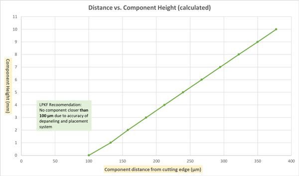
Figure 1. Minimum calculated distance of a component depending on its height for green nanosecond laser.
Considering some degree of certainty, a ratio of 1:10 for the distance-to-cutting channel in relation to the height of the component can be considered a rule of thumb.
Mechanical and thermal stress. One of the main concerns for traditional depaneling processes such as manual separation, milling and sawing is the induced mechanical stress and its potential danger for sensitive components. Consequently, the absence of mechanical stress is widely acknowledged as one of the key advantages of the noncontact laser process. A strain gauge on the PCB substrate was used for measurements in order to further evaluate mechanical vibrations during the laser process and its potential influence. Figure 2 shows the observed acceleration with a novel cutting strategy for low to high frequencies in the x-, y- and z-axis. A critical threshold of 100g was defined as a reference value, which is representative for commonly used sensors. It is evident that during the laser process observed accelerations are significantly below a critical threshold for all the considered frequencies. Hence, there is no risk of damage due to mechanical stress.
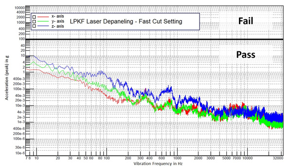
Figure 2. Measured accelerations over frequency in x-, y- and z-axis for sample layout with FastCut.
Another concern of PCB designers with laser depaneling is the potential temperatures that can occur in areas close to the cutting channel. Prior analyses have proven that these reservations are not necessary. In Figure 3 the average maximum temperatures are shown for different cutting strategies in distances varying from 100 to 500µm. The measurements have been carried out by inserting K-type thermocouple elements into the PCB substrate. For all observed distances and even in case of the closest observed distance of 100µm, the temperatures are significantly lower than the liquidus temperature of the tin/silver/copper (SAC) alloy. Consequently, the alloy cannot start to melt under any external circumstances. Furthermore, it can be observed that temperatures are decreasing significantly with growing distances, which means that even very heat-sensitive components can be placed very close to the laser cutting channel.
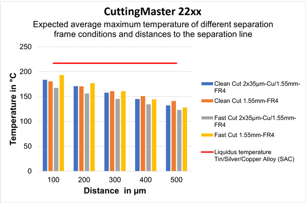
Figure 3. Average maximum temperatures for different cutting strategies, material compositions and distances to the cutting channel.
Channel widths. The laser is a flexible tool and can achieve different cutting qualities depending on the customer requirements. To enable PCB designers to lay out the panel in an appropriate way for lasers, we compared channel widths for a fast, standard and clean cutting edge. The designation is based on the quality of the cutting edge and the speed the cut is executed and is defined as follows:
- FastCut: Focus on performance and less on quality. Cutting edge is discolored and might show a slight but harmless and safe carbonization.
- StandardCut: Compromise between Fast- and CleanCut, with slight discoloration and minimal to no carbonization.
- CleanCut: Cutting edge with maximal technical cleanliness with no discoloration or carbonization but less focus on performance.
Figure 4 compares the three cutting strategies, and the qualitative differences are evident by the degree of discoloration and/or carbonization.
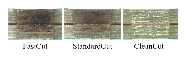
Figure 4. Comparison of cutting strategies Fast-, Standard and CleanCut with corresponding edge quality.
Figure 5 shows the width of the required cutting channel on the entry side for the laser tool depending on the material thickness of the FR-4 substrate. In general, it can be observed that the required channel width increases with thicker material thicknesses.
- FastCut: Relatively small cutting channel on the laser entry side with slight and not linear growth for increasing material thicknesses.
- StandardCut and CleanCut: Both cutting strategies require a wider cutting channel on the laser entry side which increases linear with the material thickness. CleanCut needs a slightly larger laser entry for the same material thickness.
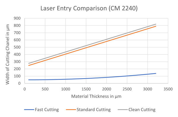
Figure 5. Width of laser cutting channel on entry side for a green nanosecond laser with Fast-, Standard and CleanCut.
As the laser beam is not equally shaped over the whole distance but tapered from top to bottom side (focus point), the laser entry and exit side have different channel widths. Figure 6 illustrates the exit comparison for the three observed cutting strategies in relation to the material thickness. Based on the results the following behavior can be seen:
- FastCut: (Relatively) very small and constant channel width on laser exit side of 35µm.
- StandardCut: Relatively high and constant channel width of around 120µm.
- CleanCut: Highest observed and constant channel width of 140µm.
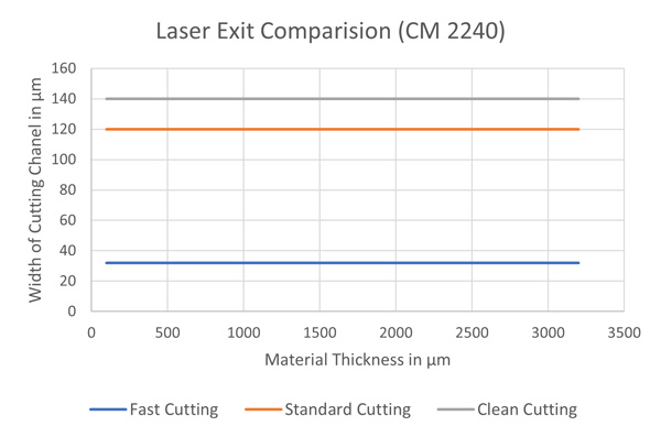
Figure 6. Width of laser cutting channel on exit side for a green nanosecond laser with Fast-, Standard and CleanCut.
The consequence of the width of the channel on the laser entry and exit side is a small angle of the PCB edge – the so-called taper. It is the difference of the widths of the cutting channel on the entry and exit side. Figure 7 shows the size of the taper relative to the substrate thickness for the cutting strategies FastCut, StandardCut and CleanCut. The following results can be observed for the different cutting strategies:
- FastCut: Relatively small taper for all material thicknesses due to a very small increase for thicker substrates.
- StandardCut and CleanCut: For both cutting strategies a comparable and relatively large taper especially for increasing material thicknesses can be observed.
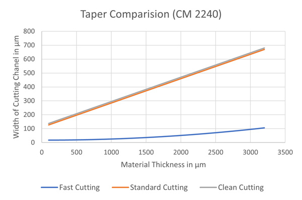
Figure 7. Taper size depending on laser-cutting strategies for an interval of material thicknesses.
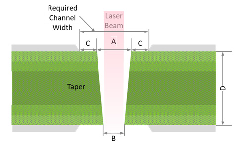
Figure 8. Schematic structure of the required cutting channel, determined by the width on the laser entrance side (A) and the twofold accuracy value (C) for a shift to the left or right.
To determine the required distance between circuit boards, not only the required laser channel but also the accuracy of the laser system need to be considered. As consequence, the required channel width is defined as follows:
Required channel width = A (width of laser entry) + 2 x C (accuracy of laser system)
It can be summarized that the desired quality or performance is decisive for the width of the cutting channel and the taper. Therefore, especially in the case of a full cut with the laser, this determines the maximum possible utilization of the panel material. In this case FastCut tends to achieve higher utilization rates.
Size and Position of Scan Fields
During laser depaneling, material is removed layer by layer by vaporizing it. With each repetition, a pulse of energy of the focused laser beam is induced into the material. Consequently, the temperature of the substrate would in principle increase with each additional repetition. To avoid this effect, usually short cooling times, called delays, are considered between two iterations.
The scan field is usually a square area in which the laser beam can be deflected without any need to move the substrate underneath (e.g., 80mm x 80mm). To achieve the best compromise of cutting quality and performance, two factors are of central importance: the size and position of scan fields on the panel. Consequently, the best results can be achieved when a PCB designer considers the effects of the size and position of the scan fields during panel layout. To better understand this, both effects are then considered on the basis of a schematic example. Figure 9 shows a potential panel design before (left) and after (right) design optimization. By adjusting the position of the tabs from the bottom and top to the sides, the number of scan fields could be reduced by two (33%). As a result, more cutting information is part of one scan field and potential delays can be reduced or even avoided.
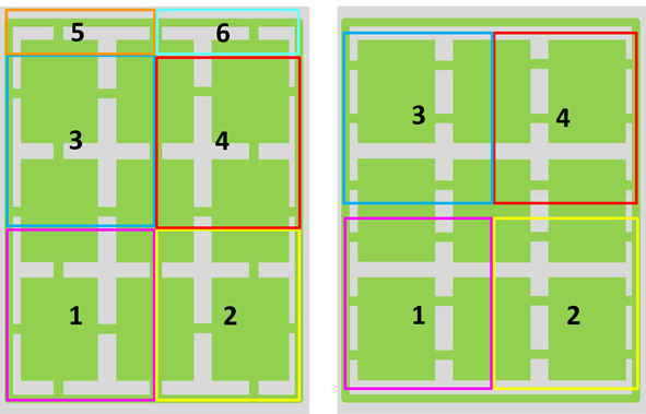
Figure 9. Schematic illustration of design optimization for laser depaneling.
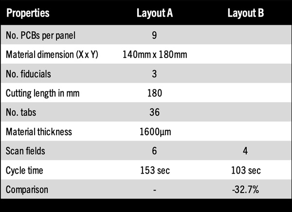
Table 1 shows the influence of the illustrated scan field reduction by optimized arrangement of tabs on a mathematical example using a calculation tool for an exemplary LPKF laser tool (green nanosecond laser). As shown in Figure 9, the tabs have simply been rearranged, with otherwise unchanged framework conditions. For each PCB four tabs with a single length of 5mm have been considered. Resulting in a total cutting length of 180mm. For those framework conditions, layout A, with six scan fields, results in a cycle time of 153 sec., while layout B, with four scan fields, requires a cycle time of only 103 sec. In total the cycle time could thereby be reduced 50 sec. – roughly a third (32.7%) of the original value. The example illustrates that even slight design optimizations might have a significant influence on the cycle time for a laser tool.
Table 1. Comparison of Sample Layout before (A) and after (B) Optimization of Tab Positioning
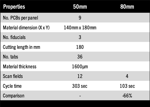
Subsequently, Table 2 shows the potential influence of the scan field size on the cutting performance and the correlation with the panel design. For the following example the cycle time was determined for the optimized layout from Figure 9 with a 50mm and 80mm scan field size. The first result is the number of scan fields required to map the panel size. For the 50mm scan field size, 12 are required, while for the 80mm size only four are needed. For the same layout, the smaller scan field size logically results in fewer cutting lengths per scan field. The effect is relatively significant for the example, so that 200 sec. – 66% of the cycle time – is saved in comparison.
Table 2. Comparison of Sample Layout with 50mm and 80mm Scan Field Size
Both examples visualize that the effect of design adjustments and scan field size can have a major impact on the cycle time of laser depaneling. This is especially true when there is relatively little cutting length, for instance due to small and few tabs.
Panel Preparation
To increase the cycle time per panel and printed circuit board, e.g., to achieve a certain clock cycle of a production line, there are multiple ways to prepare a panel by reducing the material to be cut at the end of the SMT line. Popular approaches to do so are among others pre-milling, V- and U-score. Due to the characteristics of the laser process, those preparation methods differ in terms of their efficiency. Before going into detail for each of the preparation approaches, the processes are shortly described and differentiated:
- Pre-milling: Typically performed by the PCB manufacturer, the contour of the PCB is widely mill away. The remaining material to the frame structure is also called tab(s).
- V-score: With this preparation approach the material thickness is locally reduced (in general by a third) from the top and/or bottom. This results in a V-shaped profile of the channel.
- U-score: Similar approach and generation as a V-score, but with a U-shaped or top hat channel profile.
Pre-routed tabs are a widespread approach to reduce cycle times of milling or laser tools to depanelize. Figure 10 shows a schematic illustration of a pre-routed tab with a channel width of 2.5mm. Depending on the material thickness and required panel stability for other SMT processes, the tab width can vary in the low single-digit millimeter range. In the event of mechanical separation, it also minimizes mechanical stress during depaneling. For a laser, it offers only the potential to optimize cycle times especially in combination with additional drillings. Due to the working principle of the laser, however, this does not necessarily lead to a reduction in cycle time, as it depends on other factors, which we will examine in more detail in the following.
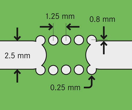
Figure 10. Schematic illustration of a pre-routed tab with additional millings for cycle time optimization.
As explained in the section on design optimizations regarding the size and position of scan fields, the target for laser depaneling is to get as many cutting lengths (cutting information) as possible in one scan field. The reason for this is to reduce or avoid cooling times to prevent excessive carbonization of the substrate material. Consequently, by reducing the cutting length in the scan field, the additional drillings may also result in more delays being required again. This is especially valid if there is relatively less cutting information, e.g., few and small tabs per scan field. In principle, the effect is therefore smaller or counterproductive depending on how much cutting length is present in the scan field. Due to varying pulse durations, laser powers and frequencies, this can vary depending on the laser depaneling system.
Another relatively widespread method is the so-called V-scoring, where the panel is scribed locally from one or both sides. This is particularly useful for rectangular circuit board contours, as only straight scribes can be made using this method. Figure 11 displays a schematic drawing of a groove with a reduction of the material thickness by one third each from the bottom and top.
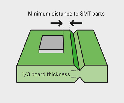
Figure 11. Schematic illustration of a V-score with reduction of the board thick to one-third.
In principle, a reduction in material thickness is beneficial to the laser, as the speed increases disproportionately for a decreasing thickness. Because fewer repetitions during ablation avoid cooling times, that could become necessary due to overheating of the material.
As Figure 12 shows, the actual effect depends on other factors: The position of the cutting channel in the scoring groove and, if applicable (in the case of preparation on both sides), the position of the grooves in relation to each other. Finally, both factors depend on the accuracy of the scoring tool. The effect of increasing inaccuracy of the scoring tool can be illustrated quite simply, since the accuracy of a laser system is relatively high, it will match the groove specified in the data with a deviation of around 20µm. However, if the groove shifts by 100µm, 200µm or even more compared with the data, the laser will not hit the groove at the lowest point but further up one of the V-shaped flanks. Figure 12 illustrates that schematic effect for a shift of roughly 100µm. While the upper groove is not cut at the lowest point but in the middle of the right flank, the lower groove would be consistent with the laser cutting channel. Accordingly, to ensure the circuit board is completely cut out, further ablation repetitions must be considered to cut through and therefore a process-reliable production.
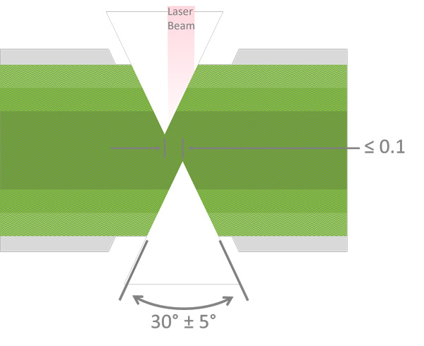
Figure 12. Offset of V-shaped grooves to each other as well as to the laser cutting channel.
With the U-groove, the approach is largely comparable to that of the V-groove, with one decisive difference in the shape of the removal profile. Figure 13 shows the schematic structure of an ablation on both sides, where the material thickness is also reduced to one-third. The characteristic U-shaped profile is clearly visible.
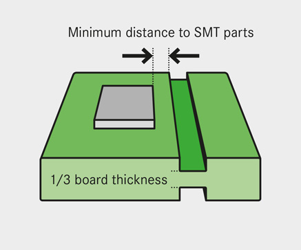
Figure 13. Schematic illustration of a U-score with reduction of the board thick to one-third.
In contrast to the V-groove, Figure 14 shows the effect of a similar offset for the U-groove. Despite an offset to the center of the scoring, the depth is constant and thus no additional repetitions need be considered. Even an offset of the upper and lower groove has no negative effect on the desired performance increase within the usual accuracy intervals of the groove tools, as the wide low points remain to overlap.
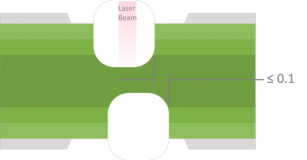
Figure 14. Offset of U-grooves to each other as well as to the laser cutting channel.
To summarize, the U-groove and pre-milled channels in particular offer a reliable increase in performance for laser depaneling. If there is a relatively large amount of cutting information in the scan field, the tabs can also be further reduced by additional drillings.
Summary
Overall, it is evident that PCB and panel design are of central importance for laser depaneling. On the one hand, potentials are revealed through placement of components on the circuit board close to the cutting channel and material savings through the relatively narrow cutting channels when the contour is fully cut. On the other hand, it shows that factors such as the cutting strategy, arrangement of tabs, the size and positioning of the scan fields and also the selection of possible panel preparation should be taken into account during the design in order to get the best possible performance and quality out of the technology.
Ed: This article was originally presented at SMTA International in October 2023 and is reprinted here with permission of the authors.
Patrick Stockbrügger is product manager SMT/PCB Production Equipment, at LPKF Laser & Electronics (lpkf.com); This email address is being protected from spambots. You need JavaScript enabled to view it.. Stephan Schmidt is former president of LPKF Laser & Electronics North America; This email address is being protected from spambots. You need JavaScript enabled to view it..