Simplify the stackups and make impedance and other measurements easier.
As many as seven different impedances are called out in various design specifications. Among these are:
- 33Ω for Rambus memory
- 50Ω for most high-speed logic
- 65Ω for the PCI bus
- 72-75Ω for analog circuits
- 85Ω differential for PCIExpress (42.5Ω single-ended)
- 95Ω differential for USB (47.5Ω single-ended)
- 100Ω differential impedance for most high-speed Internet links (50Ω single-ended)
Successfully designing a PCB with more than one of these impedances can be difficult, if not impossible. The main challenge is designing a PCB stackup that has enough routing room for all the traces of each impedance while maintaining a manufacturable, economical product. A design that is all one impedance would be of great value. If so, what impedance would be the best? Here we address this topic.
Where did all these impedances come from? It's helpful to have a sense of where the foregoing impedances came from. As seen below, their origins are diverse and the applicability of them are, in some instances, no longer viable. Below is the history of these diverse impedances.
Rambus started out making a memory system that was expected to deliver very-high transfer rates. The architecture was such that it was anticipated that the address and data buses needed to be 33Ω to function properly. The jury is still out on this, as this memory technology did not catch on, so we don't need to worry about designing this kind of transmission line into the stackup.
50Ω impedance. This has been the choice for high-speed computing since the outset since ECL and GaAs logic were employed. It matches the impedance of virtually all test equipment, making accurate measurements easy.
65Ω impedance. This was first specified for transmission lines on four-layer PCB motherboards and most game consoles. It was arrived at more or less by accident by measuring the impedance of a trace on a typical four-layer PC motherboard when it was determined that impedance control would be needed as speeds continued to increase. See Ritchey1 for a more detailed treatment of this subject.
72-75Ω impedance. Originally, TV antennas were mounted on rooftops and connected to TVs using 300Ω twin lead transmission lines. This twin lead transmission line was not shielded, so it was susceptible to noise from the surrounding environment. A shielded coaxial cable was needed to solve this problem. Since building a 300Ω coaxial cable was impractical, a 2:1 stepdown transformer was used to "transform" the impedance down to 75Ω. Ever after, this impedance cable has been used by systems that have analog signals.
85Ω differential impedance. This was arrived at by engineers at Intel who determined that the bit error rate would be lower with an 85Ω differential impedance than with a 100Ω differential impedance. This has proved untrue and later in this article we show that differential impedances are not necessary in PCBs.
95Ω differential impedance. This impedance was derived by measuring a number of USB cables and discovering that their differential impedance centered around 95Ω.
100Ω differential impedance. The early Internet was connected by twisted pairs that were obtained from phone suppliers. Originally, the twisted pairs already in buildings to connect phones were used to connect PCs and other terminal devices to routers, switches and hubs. Because the differential impedance of these twisted pairs happened to be about 100Ω, this began to be widely used in the industry.
Observations about Differential Pairs Routed on a PCB
When members of a differential pair are routed over a plane on a PCB, the primary partner is the plane over which each signal is routed. In Ritchey,2 it is seen that each side of a differential pair is, in fact, a single-ended signal parallel terminated in the single-ended line impedance. From this architecture came the idea that tight coupling is a good idea. The reality is just the opposite.
Tight coupling carries with it a number of negative side effects. Among these is that when one trace is routed very close to another one, each drives down the impedance of the other, requiring that the traces be narrowed to get back to the original target impedance, driving up copper loss. A further negative effect is that the traces cannot be separated to route through a pin field such as a 1mm pitch BGA without suffering very large impedance changes.
For those product developers who remain unconvinced there is no need to route differential pairs with a differential impedance and tight coupling on a PCB, tour any conference and look at the demonstration setups in many of the booths. Differential pairs will be connected with a separate 50Ω coaxial cable, often very far apart. All the energy spent trying to demonstrate some benefit to tight coupling has no real value. Designs we do every day with data rates as high as 32Gb/s are done to the "not closer than" rule to avoid unwanted interaction between the two members of a differential pair.
From the above discussion, it should be clear that each member of a differential pair, when routed on a PCB, is a single-ended signal parallel terminated in the line impedance and there is no benefit to tightly routing them to each other.
Selecting an Impedance
If it is possible to route all the signals on a PCB to only one impedance, what would be the best impedance to choose? From the above discussion, all signals routed on a PCB are, in fact, single-ended, even if their use is for differential signaling. Since all the test equipment we have available to make measurements is designed with input and output impedances of 50Ω and their connecting cables are 50Ω, it turns out to be a good target impedance.
Figure 1 depicts the simulation of a typical PCI driver connected to a 50Ω transmission line. Figure 2 is a simulation of the same typical PCI driver connected to a 65Ω transmission line. As can be seen, there is very little difference in the signal, so designing PCI buses with 50Ω transmission lines is acceptable.
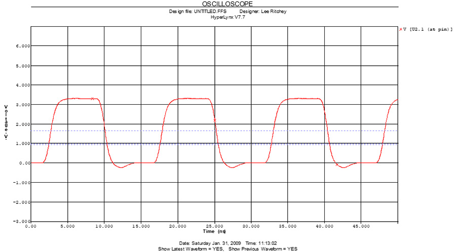
Figure 1. PCI driver simulation driving a 50Ω transmission line.
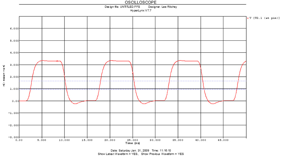
Figure 2. PCI driver simulation driving a 65Ω transmission line.
The primary application of 72-75Ω transmission lines is driving or receiving signals from an outside signal source such as a TV or some antenna. These signals are nearly always terminated on a device at the edge of the PCB. The length of the connection is short. If this connection is done with a 50Ω trace, there will be an impedance discontinuity. Rarely will this short discontinuity result in a significant degradation of the signal. If there is concern that this discontinuity will be a problem, simulation of the signal path with the two different impedances can be done. Rarely will this turn out to be a problem. As a result, 72-75Ω traces are not necessary.
The 85Ω differential impedance is really two 42.5Ω single-ended transmission lines. As noted earlier, this odd impedance is of no benefit, so routing these nets as two 50Ω lines is acceptable and, in essence, preferred.
The 95Ω differential impedance, which is two 47.5Ω single-ended lines in the USB standard, has a tolerance of +/-15%. Using this tolerance, the single-ended impedance can range from 40.375 to 54.625Ω, so a 50Ω transmission line will satisfy the standard.
Earlier it was pointed out that a 100Ω differential impedance is achieved by using two 50Ω single-ended transmission lines. Designing a PCB stackup using only 50Ω transmission lines greatly simplifies the process and also ensures that verifying the impedance is correct at the end of the PCB production line.
Conclusion
All the high-speed protocols listed in this article, except Rambus, can be successfully implemented using 50Ω transmission lines. This greatly simplifies designing PCB stackups and makes impedance and other measurements easier.
References
- Lee Ritchey, "Why is the PCI Bus Impedance Specification 65Ω?" Speeding Edge white paper, 2009.
- Lee Ritchey, "Does Differential Signaling Require 100Ω Differential Impedance?" Speeding Edge white paper, December 2021.
- Lee Ritchey, "Is Tight or Loose Coupling Best for Differential Signaling?" PCD&F, March 2020.
LEE RITCHEY is considered one of the industry's premier authorities on high-speed PCB and system design. He is founder and president of Speeding Edge (speedingedge.com), an engineering consulting and training company; This email address is being protected from spambots. You need JavaScript enabled to view it..