The industry is moving closer to the “factory-in-a-box.”
The next evolution of 3D printing – 3D printing of electronics – is here and gaining traction. Though in its initial stages, this next leap for prototyping and additive manufacturing gets us closer to the “factory-in-a-box” eventuality. Fully functional electronic products built with multiple materials can be manufactured on a single specialty inkjet 3D printer.
Today, additive manufacturing of printed electronics such as printed circuit boards (PCBs), embedded components, printed antennas or other functional electronic elements is happening. For designers and engineers, additive manufacturing is typically used to 3D-print prototypes that can be tested and modified and printed again if needed. In a world where almost every device can be connected via Internet of Things (IoT) technology, 3D printed electronics can offer designers more freedom in their designs, accelerate the design and manufacturing process, and increase the efficiency of producing customized products.
Volume production printing is left to more traditional means. In time, that is very likely to change as well.
Additive manufacturing for printed electronics uses high-resolution inkjet printers and involves multiple materials such as breakthrough conductive and dielectric inks that can be printed simultaneously. It also involves software capable of converting complex schematics into layer-by-layer print instructions.
This article examines the elements involved in this coming tsunami of additive manufacturing, and explores the benefits, challenges and the promise. First, we’ll examine the physical components needed. 3D printers capable of producing circuitry. Printers used in professional printed electronics are complex because they must be capable of 3D-printing multilayer circuits, PCBs and more, using multiple materials. Often the internal ordering process for a normal PCB prototype can take many days or even weeks in large security-focused organizations. Systems in this category are designed so designers and engineers can build functional, multilayer circuit boards, antennas and other printed circuits in-house – in a matter of hours.
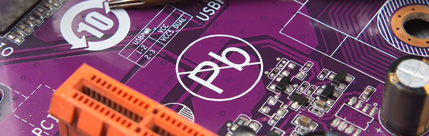
Additive manufacturing for electronics gives designers options for replacing conventional subtractive manufacturing of prototypes of PCBs, an expensive, time-consuming, multi-stage, labor- and material-intensive process. With in-house printers, designers can generate multilayer electronics – including all interconnections between layers – on a printer that applies inks in nanoparticle layers (FIGURE 1). These specialized printers work with sophisticated proprietary software that helps manage the precise printing process, which is described later in this article. With all this in place, designers can print electronics, test them on the fly, and even modify their designs and explore new geometrically complicated circuitry such as odd shapes, flexible substrates and more. The result is increased quality of design and/or faster designs and shorter design cycles.
Unlike traditional printing of circuits, 3D printers work on three axes: x, y and z. The printers must be able to print thickness-relevant elements such as vias, interconnections and through-holes during the print process.
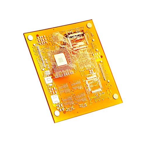
Figure 1. Multilayer 3D printed board, printed on Nano-Dimension Dragonfly 2020 3D printer.
New materials. Typical inks used for this type of inkjet deposition printing are highly conductive silver nanoparticle inks. Also needed are nonconductive, insulting dielectric inks that are compatible with the conductive ink and ensure adhesion, thermal dissipation and more. These “liquid metal” inks contain particles ranging in size from 10 to 100-plus nm. The printer must be able to deposit and cure or sinter these inks to meet the requirements of what is being printed.
These advanced materials must provide exceptionally reliable printability and outstanding electrical properties, thus offering significant time and cost benefits over traditional processes used to produce functional electronic devices.
Attributes to look for include inks that sinter at low temperatures and that can work with a variety of substrates such as paper, polymers or glass, perhaps requiring coatings to prime the surface. Manufacturers of these specialty inks often offer custom ink formulations for specific printing processes and applications that enhance adhesion, flexibility and other mechanical properties. These purpose-built inks are important for those who may want to use additive manufacturing for printing RFID, OLED lighting, circuits, screen bezels, solar, sensors and other applications requiring high conductivity for applications in defense, aerospace, automotive, telecom, medical, industrial and consumer electronics.
For designers, digital inkjet printing with specialty inks offers many advantages over screen printing and other analog options traditionally used for printed electronics, including these benefits that come about because the printer is used in-house:
- Elimination of setup costs as well as lowered operating costs.
- The ability to produce with less material and through a cleaner, more environmentally friendly, virtually waste-free process.
- A more flexible and precise production process.
- Enough speed for prototyping and iterative design.
- The ability to affordably create custom, multi-material, complex parts, which in time will lead to low-volume production.
Specialty software. Regardless of the type of 3D printer, it won’t be of much use without the right software. Moving from customary software formats – such as Gerber, VIA and DRILL files – to printed electronics is not possible without software that enables preparation of production files of 3D printed electronic circuits on the printer.
Such advanced software permits management, editing and printing of electronics files. One such software package, for example, presents a unique interface that displays Gerber files and an accurate and detailed description of the PCB’s structure, which facilitates a highly precise conversion to a 3D file format. With software like this, users of these specialty 3D printers can easily edit and prepare multilayer 3D files for printing (FIGURE 2).
Considerations for software should include the ability to adjust the many parameters needed for additive manufacturing of electronic elements, such as layer thickness, conductor width, layer order, punching and rotation options, as well as the shape or object outline. In addition, the software should permit optimization of the printing process by maximizing use of the printing surface. And it should allow the engineer to create the production files for automated additive printing, with no intermediate files, so the switch between Gerber to 3D files is seamless.
Benefits for Designers and Fabricators
A US Department of Commerce study in 2011 pointed out that intellectual property (IP) “theft costs domestic industries an estimated $200 billion to $250 billion a year. This robs American workers of hundreds of thousands of jobs.”
That data are just from the US, and were from nearly six years ago. The risk of IP theft remains high, and it’s one of the primary reasons many companies are eager to print their own electronic prototypes in-house. By eliminating the need for outside – often overseas – prototyping facilities, the IP is better protected.
Time and quality is another benefit. Prototyping or printing small quantities in-house with additive manufacturing lets designers both increase the quality of their designs, as well as enjoy faster design development and shorter design cycles. This is the result of earlier access to functional prototypes and the ability for more frequent redesigns. The overall design cycle is reduced by lowering the lead times of whatever is being printed. While typical lead times for PCB suppliers in Europe and Asia start at eight working days for medium-complex PCBs, the lead time easily can climb to 50 working days for complex designs. With an in-house solution, prototyping can take eight to 12 hours, depending on the size and complexity of a board, which is often 10 to 15 times faster than ordering PCB or other electronic component prototypes the traditional way.
For companies, the ability to save time and protect IP translates into saved money and increased competitiveness. Rather than prototyping through a service – with potentially expensive back-and-forth iterations – in-house printing offers the benefits of agile and iterative designs, and reduces PCB design and test cycles from months or weeks to days or hours. It also makes it possible to inexpensively evaluate design alternatives and creative ideas. Other cost savings come by eliminating the setup costs associated with prototyping facilities, which often charge on-time fees of hundreds of dollars for the service.
Moreover, additive manufacturing for electronics remains a greener alternative to standard PCB production since it is a cleaner process with no waste.
Challenges
While the world of additive manufacturing for electronics is evolving quickly, challenges remain. Perhaps the greatest challenge is speed. Until printers can generate fully-functioning electronic elements quickly, the printers will likely continue to serve as resources for small-quantity printing and prototyping. While even those benefits are being proven daily by early adoptees of these specialty inkjet printers, vendors are working diligently to improve and speed the process so it will be possible to print in greater quantities.
Beyond print speeds, it is also crucial that the materials used are proven to meet the stringent requirements of inkjet printing, and that they will have the same longevity of life as materials used through traditional printing methods.
Another challenge involves meeting the needs of designers and manufacturers who want flexibility and creativity in their final designs. That means additive manufacturing will need to enable printing many steps and materials into one print job to significantly increase opportunities for complexity beyond what anyone has imagined today. When 3D printers are used for solving design and functionality issues, the greater the contribution of additive manufacturing.
As the technology continues to mature, the 3D printing industry may need to consider introducing or endorsing standards around ink specifications or software for converting Gerber files, so that quality is not overlooked as more players enter the arena.
While we’re already seeing growth in the consumer 3D printing space – particularly as prices come down – the future is really going to be about additive manufacturing for industry. The industry is already jumping aboard with companies including PHYTEC and Harris using the technology, and manufacturers such as GE, Siemens Ford and others are focusing on bringing 3D solutions into their factories.
Other companies established in contract manufacturing are studying ways to use additive manufacturing to improve manufacturing operations, asking questions such as, Can we 3D-print part of the manufacturing process? Production line efficiency and flexibility moving forward will almost certainly require 3D printing to be used in either the end-product or as part of the machine making the end part, or both. The wider logistics chain also will be a beneficiary of this innovative technology. If one considers the SAP Ariba business-to-business marketplace, for example, it’s not a stretch to imagine them offering parts printed through additive manufacturing to enable truly just-in-time (JIT) custom manufacturing. For warehousing and shipping, additive manufacturing could bring about changes in the complexity of operations as more people print the parts they need in-house, as they need them.
In the foreseeable future, additional impacts will be felt with the addition of greater flexibility in combining materials – perhaps different metals, or with metals and polymers or metals and ceramics – in the same print job. Multi-material capabilities will give designers new freedom to begin deploying additional functionality within parts, such as electrical capabilities to mechanical objects. In the end, this capability will bring about stronger, smarter and more functional final products.
The industry also will have to address printing speeds and size issues, which will open new doors and industry adoption. With faster printing, multiple materials and the integration of functioning electronic circuits, the possibilities for industries deploying 3D printing are nearly limitless.
Simon Fried is chief business officer, director and cofounder of Nano Dimension (nano-di.com); This email address is being protected from spambots. You need JavaScript enabled to view it.. He will speak at PCB West in September.