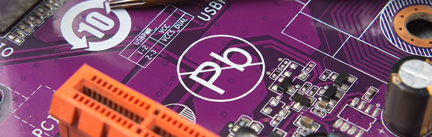
Innovative solutions based on new materials, hybrid circuit board assemblies with various technologies and embedded circuits
Leoben, June 19, 2018 - With significantly higher data rates and quantities as well as high power densities increase, the demands on the joining technology. Here can be indisputably the new 5G-generation mobile communications as an overarching and determining trend make, with applications that the infrastructure (base stations), devices (mobile phones), but also relate to use in real-time automation applications. AT & S supports the current introduction of the 5G-generation mobile communications with RF optimized connectivity solutions and will offer appropriate solutions for the further development of the new standard.
The introduction of the 5G-generation mobile communications has far-reaching consequences on the product and system-level in terms of miniaturization, functional integration, EMC and signal integrity, modularity, safety, security, etc. Against this background, AT & S has the customer requirements and the impact on the printed circuit board analyzed substrates and packaging and initiated such developments or implemented. The answer to the challenges of 5G are innovative solutions, including new materials, the combination of different technologies for hybrid PCB assemblies or the embedding of passive and active circuit components. For it was not only invests in processes and materials, but also to corresponding RF test solutions in order to investigate, for example, transmission losses, phase shifts and signal delays up to 100 GHz.
The introduction of the new 5G-generation mobile radio frequency bands with up to 6 GHz is already underway. In the next step 5-G-millimeter wave should then come up with frequencies of 28 GHz or even higher. Basically, this means to reduce for a connection technology manufacturers such as AT & S, signal losses and disorders by, for example, the dielectric with respect to the material (dielectric constant) or the thickness, the material transitions (interfaces) or the copper roughness are optimized.
With respect to the copper, the major challenge is that less rough copper for RF applications has advantages though, but a slightly higher roughness for adhesion of the conductors to the base material is necessary. Against this background, AT & S has examined the available on the market copper foils for RF applications such as 5G intensive. The geometry (profile) of the interconnects has a higher frequency on signal delays and must be optimized. Moreover, it also examines the effects of various metals (copper, gold, nickel) at AT & S to each other with respect to the skin effect in the GHz range, and accordingly developed new surface materials for its ideal use.
For 5G applications provides a hybrid circuit board assembly with the combination of high-speed layers (RF optimized) and standard layers a performance and cost-optimized solution. Thus, AT & S has realized a 12-ply hybrid Board (HF and FR4 in 2.5 D) technology for radio systems with fully integrated RF antenna. The connection of the layers takes place via Micro-vias (filled and stacked). Another exemplary RF optimized solution represents a 6-layer board that HF-layer combined with a very low dielectric constant and embedded components (ASIC of the antenna structure). The connection between the ASIC and antenna via laser vias.
AT & S Austria Technologie & Systemtechnik Aktiengesellschaft - First choice for advanced applications
AT & S is the European leader and one of the world's leading manufacturer of premium PCBs and IC substrates. AT & S industrialized pioneering technologies for its core businesses Mobile Devices & substrate, Automotive, Industrial, Medical and Advanced Packaging. AT & S has a global presence with manufacturing facilities in Austria (Leoben, Fehring) and one each in India (Nanjangud), China (Shanghai, Chongqing) and Korea (Ansan, near Seoul) and employed in the financial year 2017/18 some 10,000 employees. For more information visit www.ats.net
Register now for PCB WEST, the largest trade show for the printed circuit and electronics industry in the Silicon Valley! Coming Sept. 11-13 to the Santa Clara Convention Center.