Keep power and ground impedance as close as possible.
Capacitors are amazing little devices. They keep our camera flashes flashing, our stun guns stunning, our electric motors starting, and our stereos thumping. And on a PCB, they keep our ones 1-ing and our zeros 0-ing. Capacitors form the backbone of PCB power distribution networks (PDNs), and high-speed digital devices wouldn’t work without them. Not only do capacitors provide high-frequency energy to ICs, but they also provide AC return current paths for the signals travelling between them. But they can be rendered much less useful – and sometimes useless – if not properly mounted to the board.
You’ve probably seen the design guidelines that show capacitor mountings as good, better and best. “Don’t connect your capacitors with long traces.” Well, how long is too long? And how much better is “better?” The answers vary somewhat depending on the specific PCB, of course, but I set out to analyze some of the more common situations and actually quantify them.
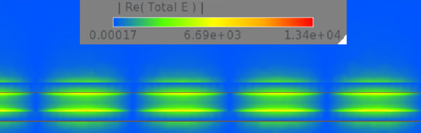
I created a test board (Figure 1) that was 10" by 10" and connected an array of 100 0402 capacitors, and analyzed the properties of different mountings.

The type 0402 is one of the more common high-frequency capacitor sizes, and I used 0.22µF capacitors. A more common value might be 0.1µF, but it is generally a good idea to use the largest capacitance available for a given capacitor body size. The reason is that the inductance of the mounted capacitor is the limiting factor for its performance, and capacitors with smaller bodies have lower inductance. So, for a given body size, or inductance, the greatest capacitance will produce the lowest impedance over the widest frequency range possible. If there were such a thing as 1000µF 0402 capacitors, those would be the caps to use!
The main goal of PDN design is to minimize the impedance between power and ground, across a range of frequencies. In the high-frequency world, the greater the capacitance between power and ground, the lower the impedance. The lower the inductance between power and ground, the lower the impedance. Since 0402 caps are small, they have a low inductance. However, their small size also limits the amount of capacitance that can be crammed inside them, so you need to use a large number of them in parallel to get a large capacitance.
To analyze the impedance of our network of capacitors, we can use an analysis tool to generate an impedance plot, or Z-parameter, of our power distribution network. I started by analyzing the impedance of the test board with the caps connected to the power and ground vias by 5 mil traces that were 50 mils long. This is the top capacitor mounting configuration shown in Figure 1. The impedance plot is shown in blue in Figure 2.

In an attempt to reduce the inductance of that trace connection, I widened those traces from 5 mils to 20 mils. The resulting impedance plot is shown in pink in Figure 2. Basically, there was only marginal improvement. The main problem with that configuration is the distance between the vias, as it creates a large loop area for the connection between power and ground. So for my next configuration, I moved the vias as close as possible, using a via-in-pad configuration. The resulting change is shown in the red impedance plot in Figure 2, which is nearly an order of magnitude lower impedance above 10MHz.
It is important to note that this analysis was done using what is called lumped analysis. This kind of analysis can be performed with a spreadsheet or other simple PI tool, and it basically lumps all the capacitors and board capacitance into a single node. It is a good planning tool, but its limitations should be understood. A PI tool that can use actual board geometries for the traces, vias and planes connected to the capacitor will give valuable data on the mounted performance of a capacitor. This is what was used in the lumped analysis. However, beyond the mounted parasitics are other parasitics associated with the capacitor(s) connection to the IC. To include these effects, perform a distributed analysis, which looks at the PDN impedance at the IC location. In Figure 2, the orange waveform is the result of a distributed analysis with the via-in-pad capacitors. The results look much worse than the lumped results (in red).
How can we improve these results? As noted, mounting is only part of the capacitor’s effect on the PDN from the standpoint of the IC. To minimize the PDN impedance, the entire loop area, and hence inductance, between the capacitor and IC must be minimized. In this case, the capacitors were connected to the planes on Layer 3 and Layer 6 of the stackup, which are spaced very far apart (in this case 36 mils), as shown in Figure 1. This is actually a very common practice in 6-layer board stackups, and as can be seen, the results are very poor. If the capacitor were instead connected to Layer 6 and Layer 7, which are only 3 mils apart, the results are improved dramatically (Figure 3, green plot). Although that change results in longer via connections to the planes (compared to the orange plot), the reduced plane separation creates a much lower impedance path to the IC. If the capacitor is instead connected to the planes on Layers 2 and 3, the via connection distances are made shorter, resulting in a marginal improvement (the light blue plot). Here you can see the importance of close power/ground spacing in the stackup. Even further improvements can be made by connecting all the power/ground planes in parallel (shown in yellow).

Can further improvements be made? Employing some PI-specific technologies, which usually incur an additional cost, can also help. For instance, using reverse aspect ratio capacitors, such as 0204s, can make the mounting inductance even smaller (shown in gray). Use of dedicated board capacitance materials that are very thin (>1 mil) with very high dielectric constants can also help by providing additional decoupling capacitance, as well as shrinking the loop inductances. For my sample board, I replaced the 3-mil dielectrics with 0.3-mil dielectrics with a Dk of 16 and saw substantial improvement in the PDN impedance (shown in white).
In summary, maximizing capacitor effectiveness is all about keeping power and ground as close as possible. Vias connecting capacitors should be as close as possible, and connected to a plane pair that is as close as possible. Doing these simple things in your PCB design will keep the capacitors happy and productive.
Patrick Carrier is product manager for high-speed PCB analysis tools at Mentor Graphics (mentor.com); This email address is being protected from spambots. You need JavaScript enabled to view it..