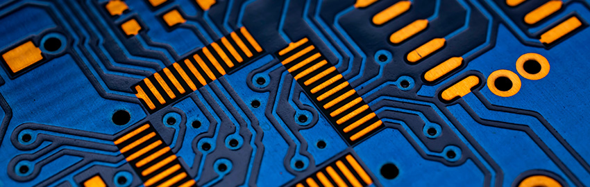
Unnecessary components or constraints can ruin board manufacturability.
Would you pack three suitcases for a vacation when everything you need will fit into two? Have you ever made one of your signature dishes without tasting and seasoning along the way?
Some folks probably do things this way since these things aren’t hard or necessarily costly to fix. It’s easy enough to shell out another $25 to check an extra suitcase, or decide it might be a good day to feed the garbage disposal and order a pizza. Such fixes have small costs. Regrettably, the smallest error on a PCB design can cost thousands of dollars to correct.
PCB designers work on a budget for both time and costs. We can’t afford time delays that come from poor planning, taking shortcuts or absorbing the cost of having boards fabricated that end up in the recycle bin. Every decision has a cost.
Here, I’m going to briefly talk about some design practices PCB designers should be using to not just achieve a quality design, but ensure it is manufacturable and testable. A good DfMA (design for manufacturability and assembly) process should be used throughout every aspect of the design flow to ensure product designs are formally evaluated, ensure the lowest possible product cost, promote the fastest possible process cycle time and achieve the highest possible fabrication yields. When DfMA is considered throughout the design flow, it helps ensure the PCB manufacturing and assembly goes smoothly, stays on schedule and the end-product is of the highest quality and reliability.
Is your design overweight? This may seem like a no-brainer, but have you actually ensured all the parts in the design are necessary to meet the functional specifications? I can’t tell you how many schematics I’ve worked with over the years where a design engineer placed a boatload of bypass and bulk caps on a schematic page, wanting them “distributed.” If you don’t need them, give them back!
Experienced designers know how and when to properly decouple circuit elements. Once achieved, removing unneeded ones saves board real estate and cost. Those nickels and dimes add up on mass-produced product. Over 10 million FitBits were sold in 2014 alone. If just two 0603 capacitors at a cost of $0.005 could be eliminated, the savings would be more than $100,000. Imagine how quickly those fractions of a penny would add up for the 230 million iPhones sold in 2015.
Are your constraints constraining you? Creating constraints for a PCB design can ensure necessary rules are followed during placement, fanout and routing. Defining constraints for items like component-to-component spacing, trace-to-trace, etc. through all types of signal integrity rules is all-important to ensure the PCB is functional and can be fabricated and tested. So, can a PCB design be over-constrained? If so, what issues does it create for the designer, and subsequently, is it possible to orchestrate and apply design constraints in such a way that the design does not get bogged down?
Overly constrained designs can contribute to missing critical deadlines. Two important things to consider with constraints are constrain only what must be constrained, and have a PCB design strategy that ensures the job is completed on time. Things like optimized placement and knowing how and when to execute component fanouts are key. Take advantage of components that have pin, gate or even package swapping. Testing different routing strategies and executing interactive and autorouting such that you optimize routing channels can help ensure PCB design success.
Virtual prototype: try before you buy. Running design rule checks (DRCs) prior to PCB design fabrication today is also a no-brainer, but physical interference checks, particularly with regard to component z-axis height and interference with mating mezzanine cards, mechanical components and the enclosure, are not.
Sure, most PCB layout tools allow entering component heights with tolerances; some even facilitate keep-out areas in the z-axis, but neither can accomplish what multi-board or true MCAD collaboration can. If the PCB design tool supports collaboration with MCAD tools, unexpected interferences with component heights can be avoided. Importing items like the mounting hardware, heat sinks, brackets, enclosures, etc. allows detection and correction of issues that may not otherwise have been discovered until after the PCB has been fabricated or installed.
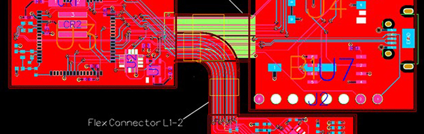
Testing 1, 2, 3. Is a testable design the best-able design? Throughout the layout phase facilitate the design for testing (FIGURE 1). The effectiveness of test processes needs to be both understood and directly contribute to identifying process defects that will improve product quality and eliminate field failures. Today, more test strategies place emphasis on functional test rather than in-circuit test. ICT (white box testing), or nonfunctional testing – in which an electrical probe tests the populated PCB checks for shorts, opens, resistance, capacitance, and other basic quantities – is to ensure the assembly was correctly made. Functional tests (black box testing) are designed to ensure circuitry functions within specifications, and are typically done “at speed” typically through connectors and/or a test fixture. The number of spring pins (also known as pogo pins) needed for the functional test fixture is significantly less than the ICT bed-of-nails (BoN) fixture. PCB designers can provide engineering design teams with extensive knowledge of PCB testing equipment capabilities, application techniques and DfT limitations.

Figure 1. Is your board testable?
Solder paste stencil aspect ratios. As smaller components are used in products requiring smaller stencil apertures, the area of the aperture opening and area of the aperture walls have become closer, requiring use of the area ratio rule in stencil design. For example, super small passives like 01005 chips can present challenges with tapes, feeders, ESD, nozzle contamination and with speed and even issues regarding placement accuracy, pick issues and placement order. Tiny 01005 chips in a nozzle are so small and thin that during pick-and-place, they increase the possibility the nozzle will come in contact with the paste. PCB designers understand the importance of solder paste aspect ratios, and typically have a good understanding of IPC-7525 guidelines, but also must know when to take other parameters and past experience into account.
Say No! to tweaking. Today there is a 90% probability there is some level of signal integrity to address on a given design. When manufacturers run their own DfMA checks, they look for ways to ensure they are fabricated economically with regard to cost and materials. What is not desirable is for the fabricator to compromise the integrity of design that fully passes the ECAD tool’s DRC and high-speed constraints by tweaking it. Communicate with the board fabricator as needed throughout the design process. Supplying the controlled impedance stackup can prevent unexpected tweaking.
John McMillan is product marketing manager at Mentor Graphics (mentor.com); This email address is being protected from spambots. You need JavaScript enabled to view it..