Many nonconductive inks have CTE and TG values that more closely match the board material.
As recently as 2000, filling a via was considered a specialty process limited to a small group of product applications and almost exclusively to one material: conductive ink. Furthermore, this process was dominated by one primary filling material, DuPont CB100. The through-hole vias were filled so that a copper cap could be plated over the via surface to create a solderable land on top of the via, and thus “via-in-pad.”
This process enhanced the reliability of blind and buried vias formed during sequential lamination of subassemblies. A fully filled via prevented air, moisture or gas entrapment in the via that could later expand during thermal cycles and result in delamination or barrel cracks.
We also learned a filled via would prevent chemicals from seeping into these blind/buried vias during manufacturing or assembly. Such seepage could potentially attack or otherwise compromise the copper plating.
When it was introduced, via fill was used for high-reliability end-products. Over the past 10 to 15 years, however, the reasons to fill vias have greatly expanded, as has the range of market sectors in which the technique is employed. As package sizes get smaller, more designs require via-in-pad. This is why demand for via filling has increased.
We also have seen the emergence of alternatives to DuPont CB100. Depending on the application and market sector, some have proved to be as good or even better suited to the product’s design and application.
Today there are also other effective conductive inks on the market; Tatsuta, for example, is one that uses copper for conductive particles, rather than the silver found in CB100. (Keep in mind these inks are being used to fill copper-plated holes.) It costs less (copper content vs. silver), and in our experience provides excellent performance and reliability.
Now let’s consider the example of two different via structures on one PCB. One uses conductive ink for via fill, and the other nonconductive ink. For a decade we’ve been debating why or when to select a conductive ink over a nonconductive ink for via fill.
Originally, it was believed conductive inks were required to effectively plate a copper cap over the via, and early on there was some validity to this point of view.
Again, in our experience, nonconductive inks such as San-Eli and Peters have clearly demonstrated compatibility with metallization. They lend themselves to a well-bonded copper cap, plated over the ink surface (via-in-pad). This is facilitated by a fortunate coefficient of expansion compatibility between the copper and the nonconductive fill.
Some believed conductive inks provided a redundant connection which would act as security for defective vias, and that the presence of conductive particles in the ink added another layer of reliability and continuity in the event the copper plating in the via cracked or was otherwise compromised. Others contend the focus should be on the PCB manufacturing process to ensure reliable vias. Besides, when one measures the conductivity or the resistance of conductive via fill inks, they fall far short of performing in the role of a redundant connection. Solid copper makes a far better electrical connection.
Many nonconductive inks have CTE and TG values that more closely match the PCB material than do those of conductive inks. These nonconductive inks expand and contract at the same rate and manner as the board material. This helps limit delamination or broken vias caused by thermal expansion mismatch.
Nonconductive inks are reliable, easy to metallize (plating a cap over the top), less expensive, and quite efficient for filling small holes and microvias.
In summary, whereas conductive inks (or only specific one(s)) were once considered the only option, we now find many nonconductive inks are superior in performance, and much less expensive. They are worthy of consideration in applications where once only a limited number of brands and formulas of conductive inks were the only option.

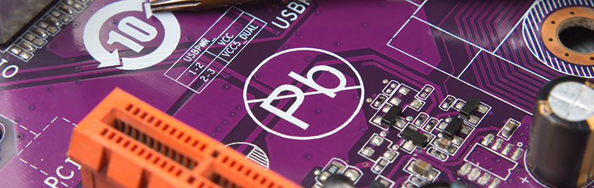
Figure 1. Nonconductive inks are proving a compatible option for via-in-pad designs.
Roy Akber is CEO of Rush PCB (rushpcb.com); This email address is being protected from spambots. You need JavaScript enabled to view it..