Designing for Higher Power in Smaller Form Factors
The redesign of a power adapter, using thermal modeling software.
Much has been written about the benefits of moving thermal design activity higher up the product development workflow to reduce the amount of rework needed later and eliminate physical prototyping for thermal reasons. That said, thermal considerations are normally indicated as advice or constraints on the main electrical and mechanical design flows.
In the case of the power adapters that NXP Semiconductors Smart Power Division is developing, thermal considerations have come to the fore, driven by trends we see in mobile power adaptors, which are getting smaller and have a higher output power. Thermal limits are now constraining all aspects of the design.
A recent project involved fitting a 25W charger into the smaller casing previously used for an 18W charger, some 26% smaller, while still meeting thermal limits that constrain the casing temperature to a maximum of 50°C averaged over an area not exceeding 2 x 2cm, against an ambient temperature of 25°C (FIGURE 1).
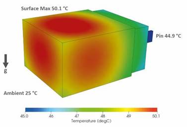
Figure 1. Thermal simulation model of the 18W charger to determine maximum power dissipation for a 25W charger.
Increasing the size of the charger, while thermally desirable, would make it inconvenient to use. Airflow through the charger, while again thermally desirable, was ruled out for safety concerns because of the mains voltage inside.
The first question we ask is, “What is possible?” This can be answered by finding out how much power dissipated within the device gives this maximum case temperature condition.
By building a simple block representation of the adapter consisting of just two blocks for the body and two for the pins, with a uniform internal power distribution, the power dissipation can be increased until the temperature limit is reached. The adapter casing and the thermal model of the ideal case with no hot spots are shown in Figure 1.
Digital simulation modeling. This simulation showed that, in theory, the adapter could dissipate a maximum of 2.7W. Given the output power needed to be 25W, the minimum efficiency, ƞ, had to be 25W/(25 + 2.7)W = 90.3%, providing a performance constraint on the electronic design.
The next step was to model the initial design of the new adapter to see the surface temperature distribution and where the temperature would exceed the limit. At 2.91W, the initial design would certainly exceed the maximum temperature, but insight into the temperature distribution in this design helps identify hot spots and guide design improvements.
To build this model, components that have a significant power dissipation were included, along with electrolytic capacitors, because these are both large, influencing the overall thermal behavior, and are temperature-sensitive (FIGURE 2).
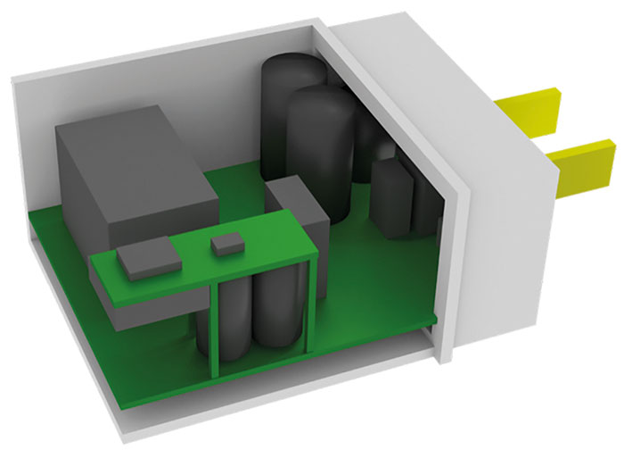
Figure 2. Initial digital block design in the 3-D thermal simulation software.
One key aspect of the electrical design is the need to isolate the high-voltage mains supply from the low-voltage output stage. This was achieved by leaving a large distance on the main PCB between the mains connected high-voltage primary side, and the output connected low-voltage secondary side. A small second PCB was added because not all secondary side components fit on the main PCB.
Each of these PCBs were expected to have four layers: two 35µm outer signal layers, and two 70µm internal power planes (mainly used for internal low-voltage supply and ground). These boards were modeled with discrete layers, but with averaged material properties for each layer, assuming 30% copper coverage for the signal layers and 70% for the power planes.
A key decision in early design is how to model the components. Most components were modeled as discrete blocks having a uniform internal power dissipation and material properties, with values chosen based on the primary material for the part.
As expected, the case temperature exceeded 50°C in several places, caused by local hot spots inside the adapter, with a maximum surface temperature of 61°C (FIGURE 3).
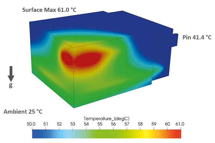
Figure 3. Thermal simulation of the initial design surface temperatures.
Addressing the hot spots. Two key hot spots inside the adapter were the primary MOSFET on the main board and the synchronous rectifier MOSFET on the small second board (FIGURE 4). Next to these two components, the transformer has a high dissipation and gets warm, but has better cooling because of its larger size.
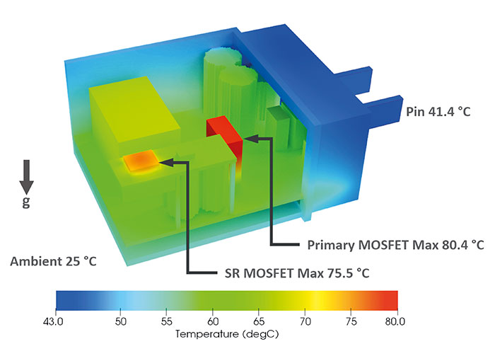
Figure 4. Hot spots from the MOSFETS inside the power adapter illustrated in the product model.
Rectifying these issues to achieve an acceptable thermal design within the deadline the customer required was a team effort, requiring close collaboration between the application engineers working on the sizing of the components and providing power estimates; the layout engineer working on the PCB layout; and the author as the thermal engineer to suggest thermal improvements and to investigate the thermal impact of these by performing 3-D digital simulations computational fluid dynamics (CFD) software.
Collaboration to build a better PCB. The process involved sitting together and listing ideas, which the author then tried out in the CFD tool. Based on the results, we decided which ideas to accept and which to reject. We went through that cycle several times, described in more detail below, resulting in the final PCB layout that was simulated and later assembled.
Because the power dissipation was known to be too high, optimization of the circuitry and control was started. We focused mainly on reducing the power dissipation in the primary MOSFET, the transformer, and the synchronous rectifier MOSFET, which was used in preference to a rectifier diode because it dissipates less power but requires a drive signal provided by the synchronous rectifier chip.
This work resulted in a total power dissipation of 2.2W, giving a 91.9% efficiency. Because this was below the 2.7W theoretical maximum, cooling should be possible, provided hot spots on the casing could be reduced. So, as well as forcing a redesign of the circuitry and control, thermal constraints also necessitated a significant redesign to alter the layout of the components to better spread the heat dissipation throughout the adapter.
Parts placement. Key changes were to move the primary MOSFET from the top of the main board to the bottom and away from the transformer to separate these dissipating sources. The primary MOSFET was mounted flat onto the PCB to conduct away more of its heat.
The four bridge diodes were then moved to the top of the main board. These changes meant that one of the large cylindrical capacitors on the main board also had to be moved. This was mounted on its side and raised off the main board.
The size of the small second board was increased to improve heat spreading, and the location of the connecting wires was changed. Between the transformer and secondary board, a vertical plastic wall was added to help conduct heat from the secondary PCB down into the main board and into the transformer, to help remove heat from the synchronous rectifier MOSFET.
The final change was to move the USB connector to the main board because the cable, which will be present when the adapter is charging and thus dissipating heat, would help remove heat from the adapter. The pins supplying mains power to the unit also would conduct heat into the mains socket. The final design changes are illustrated in FIGURE 5.
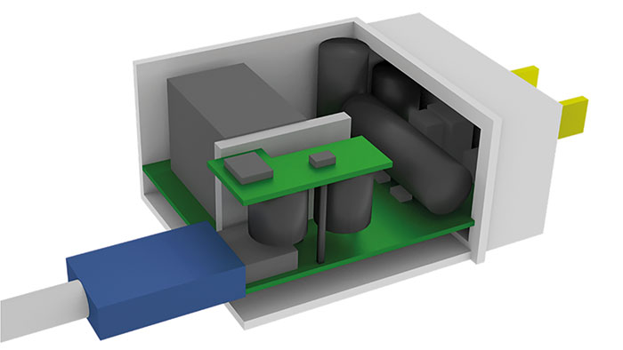
Figure 5. Digital model of the final design iteration.
These changes dropped the temperature of the casing adjacent to the synchronous rectifier MOSFET by 10°C. And with the maximum casing temperature averaged over a 2 x 2cm area of 48.8°C, as measured by a FLIR infrared camera with a USB cable attached (FIGURE 6), we met the design requirements.
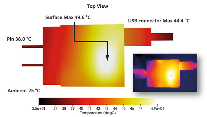
Figure 6. Surface temperature compared with measurement results of the final design.
This work illustrates the importance of thermal design for electronic products and the insights possible using 3-D digital simulation and analysis. The simulation results of the final adapter design were in close agreement with the surface temperature maximum and distribution measured on the casing after the adapter was fabricated, so no further design rework was necessary.
Had this design not met the requirements, we could increase the size of the charger slightly to improve the external cooling and use more expensive components internally or increase the copper content of the PCB. All these changes would have added cost to the final product, and the simulation software helped find what we believe is the lowest-cost, best-cooling solution for the product.
Acknowledgments
The author would like to thank Frank van Rens for the optimization of the adapter’s circuitry and control, and Thady Bruton for the thermal measurements performed on the adapter. This work was originally published as “Thermal Modelling to Optimize Design in Mobile Charging Applications” in the Proceedings of the 23rd Therminic Workshop, Amsterdam, September 2017.
is technology manager at NXP Semiconductors Smart Power Division.


