Generating PCB Footprints for Your First Layout

And why your library naming convention should be memorable.
As a designer who has put himself into the public eye, a lot of questions come my way. Several beginners have approached me with basic questions I can usually answer by sharing something I’ve already written. Sometimes I’ll end up writing a few paragraphs that eventually expand into a column to share with everyone. One gentleman, whom I will call Aakash, has leaned on me so many times I think he might be compiling a book. The messages pile up, as do the answers. Let’s get to one of those types of answers.
More than one person has asked about starting their first job going from the ground up. “How do I make all the parts I need for my first board?” The short answer is to build them one at a time. This is the internet age. This is the 21st Century. There must be a better way! It’s not that we’re impatient; we just don’t have that kind of time. Software vendors know that, and the internet does too. The software installation comes with a bevy of common parts, but most boards go well beyond the generic SMD capacitors and resistors found in the default library.
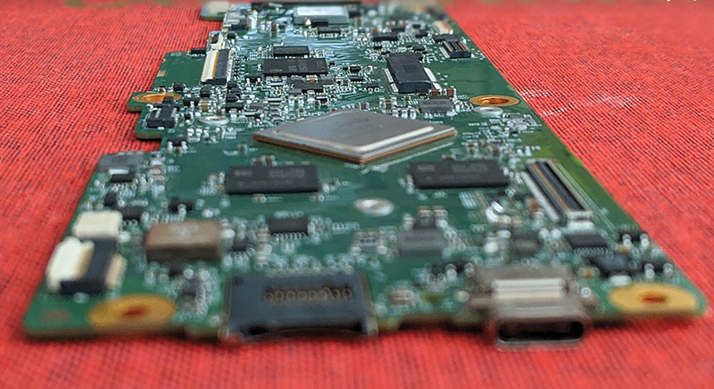
Figure 1. The PCB layout can only be as good as the underlying footprints all the way down to the padstack where it all begins.
You have it so good. In “my day” we finished a layout and saved it to a floppy disk. We walked it over to Document Control, and they put it in a file cabinet. Some veterans may be nodding. For you kids, a floppy disk looks like the icon we use for saving our designs, but that’s a story for another time. Now get off my lawn!
The library must start somewhere, and most PCB layouts start at the connector, so I’ll start there. Connectors are like snowflakes, more or less by design. You can find at least 100 different circuits that fit on a QFN-16. That’s a square with 16 pins spaced maybe a half a millimeter apart with a center ground pad. Meanwhile, every connector mates to only one other connector. An SMA connector doesn’t work with an SMB socket.
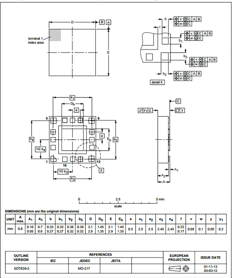
Figure 2. One of the most common SMD packages is the QFN, quad flatpack no lead, as opposed to QFP, which has gull wing leads protruding from the body. Credit: Reference Designer.
Why connector catalogs are so byzantine. Worries over patent infringement and protecting their turf work against the connector vendors. I don’t expect them to ever standardize on the particulars. The proliferation of connectors is further complicated by the way connectors are documented. You will never find a drawing of the connector you need. What you will find is a representative image used for the entire connector family. Everything from two pins to 300 is represented by that single drawing. Then you get to decode the part number to find the actual body dimensions. Up to 17 pins, it’s one row, 18 to 80 is two rows, then three and so on (FIGURE 3). Turn to some other page that indicates what the plating letter means. Another table breaks down whether there are zero, one, two or more alignment pins. Go to still another page to find out if your mating connector locks down mechanically or relies on friction. Do you want tape-and-reel? Or is a tray okay?
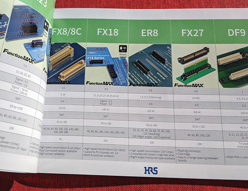
Figure 3. The 2020 Hirose pamphlet. If you want to build the part, be ready to turn some pages.
Coming to this from the component selection side is the same thing in reverse. You build that part number one character at a time. When finished, you get to contact the vendor to see if it is a standard part or if you get to wait six weeks and pay some nonrecurring engineering fees. Maybe you have to roll the dice again. All for the pleasure of buying some connectors. I just love connectors, and they’re on almost every board. I’ll try capacitive charging with an array of antennas and still get a swath of board-to-board connectors.
A brief history on library generation. Back in the era of floppy disks, I had catalogs from Amp, Samtec and others to suss out the details. The best ones were from Texas Instruments. One fine day, a new PCB designer rolled into an empty space we called a “cubicle.” As he unpacked his box, I couldn’t help but notice a large number of UPS-Brown paperbacks that were all identical except for minor variations in width. He owned the entire Encyclopedia Motorola! I didn’t even know his name, but I already liked him. Those items were a status symbol to me at least. My generation got tired of lugging all those books around, so we invented the internet.
That’s where you come in. Do you want to slog through those books and piece together a component footprint one padstack at a time? Ask your vendor(s) if they can part with more than a .pdf file and provide a CAD file in your preferred format. Some will offer files for a specific ECAD tool or a STEP model to import. Others may be old school and deal only in .dxf files. Either way, you have a leg up on starting from scratch with the “wizard.” Verifying the right geometry is still up to you.
Library naming conventions. No matter how you approach library generation, a naming convention is a must. As your library grows, it’s possible to spend more time browsing for an existing part than it would take to build it again. IPC-7351 to the rescue. Each revision of this document goes into a little more depth to cover the millions of different footprints and the various ways they will be built.
Circling back to the QFN, a typical file name is as follows: QFN50P_300x300_16_150x150. The newer revision of the document will include another character or characters to define the footprint in greater detail. The point is to stick to a system. If you’re starting with chaos for file names, then you want to make renaming your symbols part of each design effort, one board at a time. Twenty percent of the parts cover 80% of the board, so it gets easier as you go.
IPC-7351B, page 17, gives a flavor for how to create footprints in such a way they can be searched by their parameters (FIGURE 4). One of the most important characteristics is footprint size: small, medium or large. For everything but Class 3 high-reliability work, I recommend the nominal size, rather than over- or undersize footprints. If big pads present an impedance issue, or the boards are very high-density, it could be useful to minimize size. The Ghostbusters tell us to “never cross the streams”; I’m telling you to never mix the minimum, nominal and maximum size component footprint types. Bad things can happen if you commit either of those sins on the same board, especially with the same part.
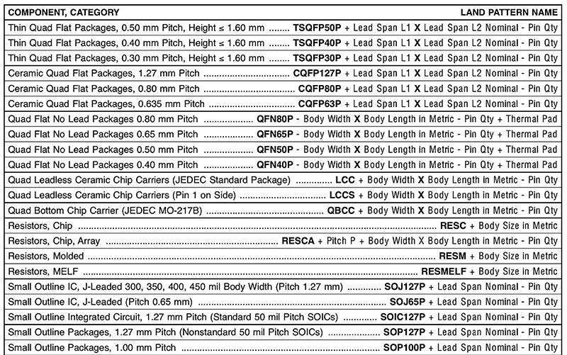
Figure 4. IPC-7351B gives a flavor for how to create footprints searchable by their parameters.
It doesn’t take a hero to curate a good library. Help is available. A number of companies will generate library parts by subscription or piecemeal. A service bureau may be willing to share its library for a nominal one-time fee. The task group chairman of the IPC naming convention standard is in the library business, and his company (PCB Libraries) is a place to start. Ultra Librarian is another that comes to mind.
You don’t have to be a hero and do it all yourself, but since the PCB is no better than the underlying library, checking every part against the data sheet is strongly recommended. At Google, we weren’t allowed to tape-out a board until every part to be used had been checked by a person not involved with the part creation. That extra pair of eyes helped prevent scrap.
A bad part can be costly. You lose money on scrap, but more important, you lose time, which you can only spend once, and it’s gone. Library symbols built incorrectly enough times can cost the company customers. Bear that in mind from the moment you open the padstack editor to create the first brick of your building. It can come crashing down that quickly. Getting off the ground starts with the basics. A good foundation for your PCB starts in the library.
is a career PCB designer experienced in military, telecom, consumer hardware and, lately, the automotive industry. Originally, he was an RF specialist but is compelled to flip the bit now and then to fill the need for high-speed digital design. He enjoys playing bass and racing bikes when he's not writing about or performing PCB layout. His column is produced by Cadence Design Systems and runs monthly.


