HELMOND, THE NETHERLANDS -- BGA component mounting on the PCB created a huge leap in innerconnect capability, but with BGAs getting much larger and pitch going below 1mm, advanced PCB densities are not keeping up with demands of the BGA packages.
Sequential buildup technology is a good technical solution but a costly one as well. To fan-out form large BGA packages requires a high volume of PCB layers.
BGA pitches moving toward 0.5mm grid cannot be routed without sequential lamination of the PCB layers. This dramatically limits PCB manufacturer selection. With higher technology in one area of the PCB (and much less everywhere else) MCM technology is being used more frequently, but can be cost-prohibitive compared to conventional PCB products. BoM and yield costs are increasing and can even be more than the component reduction cost from reducing BGA pitch on the components.
VeCS (Vertical Conductive Structure) technology is engineered to increase the densities in the vertical connections. The new patented technology is a shift from conventional drilled holes or lasered holes. It enhances power distribution in and out of the grid array and is able to route more traces in the routing channel. The reference planes offer a much more stable and constant image to the signal layers resulting in less distortion of the signal enabling higher data rates. The innerlayer P/G copper weight can also be lowered, as the reference plane width is typically 150% wider under area array packages than any drill or laser processes today. VeCS vertical connections lower inductance and capacitance compared to traditional vias. This boost can improve SI performance and make higher bandwidths possible.
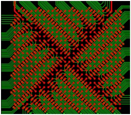
Since VeCS can route much wider signal channels, the trace width could be larger and dielectric layer thickness higher than any other innerconnect technology in the industry (compensate for skin effect). Even with HDI or MCM options, sub-0.8mm BGA manufacturing methods required dual lamination, HDI build-ups and sequential lamination small hole drilling methods. Both are higher in cost than traditional PCBs. The advantage of VeCS to BGA routing is more apparent as pitch goes below 1mm and size increases above 100 I/O. Conventional PCB manufacturing equipment and materials can be used with VeCS even for below 0.5mm BGA pitch. FIGURE 1 shows diagonal routing in the very wide channels on a 1.0mm pitch footprint.
The technology can lower the layer count of most large BGA PCBs. The topside of a PCB could have all the components placed in the same location, use the same material as the previous revision, and achieve better SI performance while lower PCB costs.
Although the technology is new to most PCB manufacturers, any medium/high technology PCB board shop can be trained to manufacture it. No new additional capital equipment for board shops is required, and NextGin will train and certify fabricators on the technology.
The process, design, and product DfM technologies are now available for each cycle of the PCB manufacturing food chain, and NextGin is actively working with the leaders in CAD software to automate the auto-route capability so new designs are created at the same speed as all conventional PCB technologies.
Two fabricators are currently manufacturing VeCS technology.
VeCS offers complete CAD design recommendations and PCB manufacturing guidelines. This email address is being protected from spambots. You need JavaScript enabled to view it. - www.nextgin-tech.com