Pros and cons of using (or not using) constraints.
A correct-by-construction methodology may appear to be a time-consuming planning task, but time taken during the layout planning can save hours or days on a schedule by preventing design mistakes that can cause product failures or hours of design rework. Proper constraint definition can make a PCB design much easier and eliminate the opportunity for errors.
When proper constraints are not used, it becomes impossible to get it right the first time. Some factors that will cause issues during design are:
- The “Human Interface.” The designer in the chair is one of the biggest reasons for errors. Not on purpose of course, but because we are all human we miss important requirements within the design phase as we worry about other requirements.
- Lack of preparation. Preparing the database at the beginning of the design is most important to keeping the design task efficient throughout.
- Rushing the design. We are all under very aggressive schedules, and rushing designs to completion can cause designers to miss requirements.
Designers are continually pushed to reduce time to market. Using proper planning of constraints can:
- Achieve high-quality designs with confidence during the design layout phase.
- Improve speed and efficiency during the design.
- Lower design costs due to less rework at the end of the design and provide for a faster release to market.
In the past (and unfortunately some designers today stick to old methods), rules were used sparingly – if at all – to route designs. Many designers still use a grid-based routing system to avoid spacing errors on their designs. Using a grid, for example, of 5 mils permits the design to be routed easily with 5 mil lines and spaces. This works if all the design requirements are for 5 mil lines, but designs of the present seldom have such simple requirements.
Another commonly used method is to design and route with DRC (design rules checking) set to disabled, allowing a designer to quickly throw etch onto a design without worry of errors. This is because the designer plans to catch and correct errors at the end of the design. That’s an irresponsible approach, as it can cost hours to days of rework, all at a time when the design should be going to fabrication.
New tools and methods are very different. Modern PCB design tools are constraint-driven, and the layout tools are shape-based, relying on properly planned constraints to drive trace routing using gridless methods. A common spreadsheet-based constraints database that is updated, whether the designer is in the schematic or the layout tool, allows both engineer and PCB designer to collaborate on constraints throughout the design. Online DRC capability allows the designer to quickly lay down etch and have the system keep errors from occurring on-the-fly, thus making end-of-design cleanup a minimal effort, if needed at all. These more-effective methods allow the designer to focus on the design, and not the errors that need to be checked at late stages in the design (FIGURE 1).
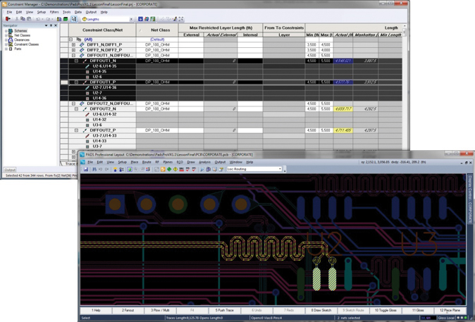
Figure 1. Once constraints are in place, routing of critical signals in the design is a no-brainer, as they are instantly verifiable to the constraints.
Constraint planning. The Human Interface is a big part of the problems that can creep into a design. We work on removing that issue by creating constraints at the planning phase of the design to help the designer work smoothly through the design without the need to check rules along the way. This is why this stage is so important, and even though it may add some additional preparation time before even one component or trace is laid, it may be the greatest increase in productivity during a design.
Set this process in motion at the earliest stages of the design. Remember: rules can exist in a design even before the board outline is drawn. In fact, some of the early constraints may have been entered into the schematic by the engineer.
In a perfect world, an engineer will provide a statement of work with all the requirements they think are critical to the design (FIGURE 2). This will help drive constraint planning and entry.
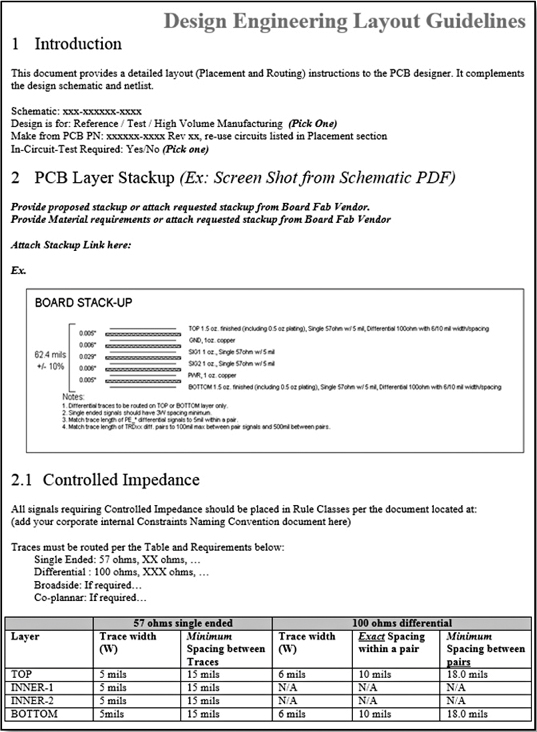
Figure 2. A good engineering statement of work, or layout guidelines, can make constraint preparation easy.
Constraint entry. Let’s look at some steps to take when entering constraints. Using this process, the designer can quickly build a set of constraints that can be trusted, and then focus on the design process itself.
- In the schematic, develop Planning/Placement Groups and circuit location information or rooms (FIGURE 3). Working with the engineer to provide placement intent that can be transferred directly from the schematic can be a huge timesaver.
- Enter all the General Clearances required within the design. These may best be developed as a baseline for all future designs, and then placed into start from templates so the data do not have to be reentered for each design. This is also a good point to develop all the package spacing requirements for the X, Y, and Z axes, so the system can flag any placement issues during 2D and 3D placement.
- Review data sheets on the chips that will be used, and check the pin pitches and sizes. This helps determine the minimum rules needed for trace width and spacing. Remember to maximize the trace width and spacing for best design for manufacturing (DfM) practices for the highest quality in-board fabrication.
- Gather the requirements for critical circuits, as other spacing, topology, delay, and impedance information will need to be input.
- Set up the minimum and maximum constraints.
- Create additional constraint clearances for known conditions (i.e., a high-speed 3W constraint).
- After all these constraints are known and set up, create schemes for exceptions. It is very important to do this last, as each scheme propagates from the default scheme. A change later will require each scheme to be revisited.
- Develop net classes for specific critical circuitry and create the class-to-class clearances to provide for spacing requirements between each critical class.
- Develop constraint classes for specific critical nets for differential pairs, topology, timing and delay matching and tolerances, etc.
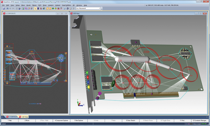
Figure 3. Planning/placement groups driven by engineering intent through the schematic allow for a quicker layout placement phase.
This is an overview, of course, but once the preparation of in-depth constraints for a design has been mastered, work will be seamless from beginning to end of the layout process without the need to check if the design meets the requirements of the engineering team.
Vern Wnek is technical marketing engineer at Mentor Graphics (mentor.com); This email address is being protected from spambots. You need JavaScript enabled to view it..